Congratulations! You're here because you want to learn the nitty-gritty details of a computer expansion bus that hasn't appeared in a new computer design for 25 years. Moreover, this bus was only used in a few systems, most notably IBM's PS/2 family of computers, but others too, including some systems from NCR.
Oh, you're still here. Hold on tight, it's quite a ride.
For the purposes of this tutorial, I'm assuming you're familiar with digital logic and computer interface buses, particularly ISA. I'll refer to ISA because it clearly influenced the design of MCA.
Let's take a look at a basic (default) bus transfer to get started. Here's a timing diagram taken from the PS/2 hardware interface technical reference manual and modified to make it more like the real timings measured on my PS/2 Model 50Z.
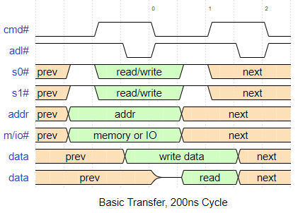
Compared with the old ISA bus, IBM made some changes to things that seem a bit pointless. The S0 and S1 status signals are just WRITE# and READ# with new names. S0 going low indicates a write, and S1 going low indicates a read. I think the reason they did this was to try and convert to a synchronous bus architecture. In this design, a new line, called CMD#, acts as the clock. READ# and WRITE# have no meaning until you reach the falling edge of CMD#.
In fact, the address lines also can be latched on the falling edge of CMD#. But here IBM made a somewhat odd design decision and added another clock! This is ADL#, the address latch. It's equivalent to the ISA bus AEN line. On the falling edge, the expansion card can latch the address lines. But this is optional, and IBM's own documentation says that they may be latched on CMD# falling. The reason for this will become clear a little bit later.
There's another control line that behaves a bit like an address line: the M/IO# line. When this is high, the address bits (all 24 or 32 of them) refer to a location in memory. But when the line is low, only 16 address bits are active and they refer to I/O space. The CPU accesses this area using the IN and OUT instructions. This control line is latched at the same time as the rest of the address lines.
Once the address has been latched, the expansion card is supposed to look at the status bits (S0 and S1) to figure out if the operation is a read or write. If it is a read, then the card puts data onto the data bus immediately, and keeps it there for as long as CMD# is low, and a little bit beyond (the data hold time). The motherboard (the planar in IBM terminology) latches the data on the rising edge of CMD#. For a write operation, the planar loads the data that it wants to write out to the card before the falling edge of CMD#, so the card can actually latch it all at once!
Going back to the ADL# line, I prefer to use it to gain some extra timing margin. In the example of my PS/2 model 50Z, it gives me about 50ns of extra quality time to spend with the address, which is useful for preparing slow-responding devices such as Yamaha sound chips.
Speaking of timing, many MCA computers use a longer cycle time for IO operations. My Model 50Z uses 300ns, such as in this diagram:
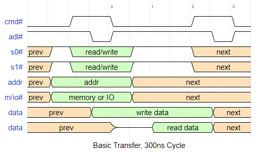
Notice that the extra 100ns is inserted in the state where CMD# is low, allowing the expansion card extra time to read or write data.
Oh and I almost forgot: There is a special line, MADE24, that must be decoded as if it is an address line, and 16-bit cards must make sure it is a '1' in their address decoder! This is to allow 16-bit cards to be forwards-compatible with 32-bit slots. A 32-bit slot has all 32 address lines, but the 16-bit card only has 24 address lines. When MADE24 is a 0, this means that the planar has loaded a 32-bit address, meaning there are upper bits that the 16-bit card cannot see! MADE24 allows the 16-bit card to see that it is not actually being addressed since the access is happening in memory above 16MB. This applies only to memory transfers, never to I/O transfers, since they always use 16-bit addresses.
IBM provided a way for expansion cards to slow down read or write operations. By deasserting the CD_CHDRY control line (channel ready) at a specific time during a transfer, the card can tell the planar that it needs more time to process the data that is on the data bus. That specific time is right before the falling edge of CMD#.
Here's a timing diagram showing a bus operation that has been slowed down in this way.
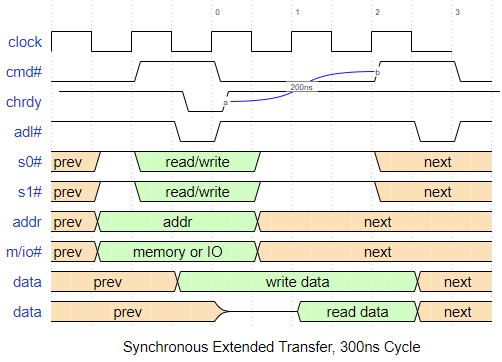
If the card asserts CD_CHRDY right after CMD# falls, then you get what IBM calls an synchronous extended cycle which has a minimum total cycle time of 300ns. But if you continue to hold CD_CHRDY low, then the planar will extend the bus cycle in increments. Oh, by the way, the increment depends on the machine! You see, the planar is actually inserting wait states which prevent the processor from accessing memory. Typically a wait state is a full processor cycle. On my Model 50Z, this is 100ns.
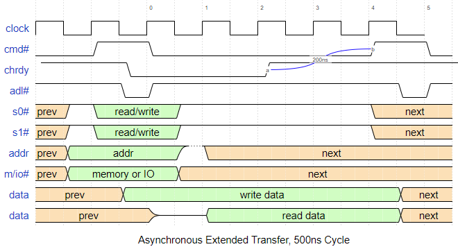
In theory you can extend a bus cycle indefinitely, but in practice, if you take too long, you'll crash the computer! IBM specifies a limit of 3.5us.
IBM produced detailed technical reference manuals for all of their PS/2 machines, and most of them have a table that indicates the bus cycle timing for that specific machine.
Conveniently, 200ns is the fastest bus transfer speed for normal MCA bus computers. The bus clock is derived from the CPU clock so it is often slower than 200ns because there may not be a nice integer divide resulting in 200ns.
These computers have multiple bus masters: the CPU, the DMA controller, and sometimes other expansion cards with that capability. Each bus master does not have to run at the same speed. For example, the Model 90 Type 2 processor complex has a 33MHz CPU with a default cycle of 240ns and a 10MHz DMA controller with a 200ns default cycle.
I've tabulated a few timings here for convenience. Timing units are in nanoseconds.
| Model | CPU Clock Period | Default Transfer | Extended Transfer |
|---|---|---|---|
| 50Z | 100 | 300 (I/O) 200 (mem) | 300 |
| 55 | 62.5 | 250 | 375 |
| 60 | 100 | 300 (I/O) 200 (mem) | 300 |
| 65 | 62.5 | 250 | 375 |
| 70 | 50 | 200 | 300 |
| 80 | 62.5, 50, or 40 | 200 or 250 (16MHz) | 300 |
| 90 | 40 | 200 | 300 |
| 95 | 40, 30 | 200 or 240 | 300 or 320 |
Notice that some computers have a different default cycle for I/O? If you only test your card on one PS/2 machine, you can run into problems because of this. If you have a slow device on your card that needs extra time, use a synchronous extended bus cycle and you will get always get a 300ns cycle time or more.
The last type of transfer is the setup transfer. IBM created this as a system for talking to one expansion card at a time. It works like a basic bus cycle but, along with the address lines, the planar asserts a special signal that is unique to each card slot. This is the CD_SETUP# signal.
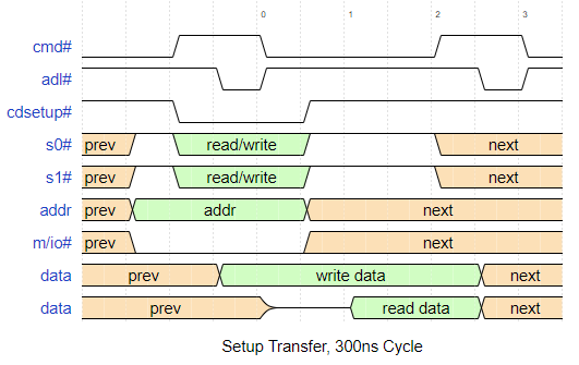
When the card sees this signal asserted when it latches the address and M/IO# lines, it looks for accesses to a special set of registers, called the programmable option select or POS registers, showing up at 0x100 to 0x107.
| Address | Register |
|---|---|
| 0x100 | Adapter ID (lsb) |
| 0x101 | Adapter ID (msb) |
| 0x102 | Option select data 1 |
| 0x103 | Option select data 2 |
| 0x104 | Option select data 3 |
| 0x105 | Option select data 4 |
| 0x106 | Subaddress extension (lsb) |
| 0x107 | Subaddress extension (msb) |
The POS registers are used during card configuration.
You might be interested to know that you can use a synchronous extended or asynchronous extended bus cycle to handle setup requests. This is useful for slow cards that use a microcontroller to implement POS functions. In fact, the adapter ID can come back as all zeros (0x0000) for up to 1 second during boot, and the BIOS won't complain!
It's time to dig into IBM's early version of plug-and-play. They didn't call it that at the time, and it certainly had its flaws. It was more like a jumperless configuration system, and it works using the POS registers discussed in the previous section.
The first two registers are a read-only and contain a 16-bit ID code that is specific to the card. To get an ID, you had to pay money to IBM and they would assign you an ID code.
The next four registers -- well, they depend on the card itself. You get to use the bits in any way you want. Each bit is like a jumper on the card. For example, you might have an "enable feature" jumper on your old ISA card. On the MCA card, this would be a bit in one of those registers. Or perhaps you had a selection of 4 different interrupt jumpers. This could be done using 2 bits that decode to 1 of 4 possible interrupt selections.
OK, there are actually three bits in those registers that are reserved and can't be used for just any old thing. Bit 0 of register 0x102 must be used to disable the expansion card. The bit defaults to 0 until the BIOS writes a 1 into the register, and then (and only then) is the card allowed to decode the address bus and do the things that it is designed to do. A disabled card can only respond to setup transfers!
The remaining two reserved bits are the "channel check" (bit 7 in 0x105) which the card sets to a '1' if there was a fault on the card. The reason this exists is because there is a control line called CHCK# that is shared by all the cards. If there is an error, like a parity error or something, then the card asserts CHCK# which triggers a non-maskable interrupt. The NMI handler needs to know which card caused the fault, so it reads register 0x105 on each card in turn to look at the channel check bit. Bit 6 of the same register tells the NMI handler if it has more fault code data in POS registers 0x106 and 0x107.
But everything else can be used by the card in any way you want! Well, except for the required fields that don't have reserved bit positions:
- Fairness enable bit: This is required only for devices that support burst-mode DMA. It defaults to 'on' but can be turned off using this POS register bit.
- Arbitration level: Basically the equivalent of the old DMA channel setting on ISA.
- ROM segment address: Any cards with on-board ROM must allow the segment address to be changed using up to 4 bits to specify 1 of 16 8KB segments.
- IO device address fields: If you can put more than one of the same kind of card in a machine, then you must be able to change the IO addresses using these fields. Seems obvious, but IBM felt the need to spell it out in their spec.
So how does the BIOS know how to configure the cards, and what the meaning of each POS bit is? The answer is that it does not know. The BIOS maintains a small area of memory in the battery-backed CMOS RAM that contains card ID values and stored values to load into each POS register of each card.
If the BIOS detects card that is not on the list in the CMOS RAM, then it asks you to boot off the reference disk. This is a special disk that contains a program that can configure the resources used by each card, and this disk is one of the big drawbacks of the microchannel architecture. Each disk was unique to each PS/2 computer and needed to be kept nearby. If you lost it, you had to get a new disk and completely reconfigure the system!
When the reference disk boots, it interrogates the cards in the system, and then it looks for an adapter description file that is specific to the card. The name of the file contains the hex value of the card ID. This is called the ADF. Inside is plain old ASCII text in a specific format that describes each field in the POS register along with the system resources used (memory/IO addresses, IRQ channels, and DMA priorities). You can get very fancy and have user-selectable options along with built-in descriptive text so that you can configure the card without having to refer to a user manual. It's quite nice.
Oh yeah, if the ADF isn't on the reference disk, the program asks for a disk that came with the expansion card which contains the ADF file. You have to do this for every card, unless you've copied the ADF file over to the reference disk. It's a pain.
Once all the ADFs are loaded, the reference disk software analyzes all the possible configuration options until it finds one that results with no conflicts between any of the cards. This is really where MCA shines and improves in ISA. However, there are situations where you can have two cards that will never work with each other due to an unresolvable configuration. The program just disables one of the cards and gives you an error.
Once it figures out a working configuration, it calculates the required POS bits for each card, and then it loads them into the cards.
The MCA bus handles interrupts only slightly differently than ISA. ISA interrupts are edge-triggered, meaning that the interrupt controller detects the interrupt when the pin transitions from high to low. It's pretty simple, but it also means that interrupts cannot be shared readily.
Say one card pulls the IRQ line low, triggering an interrupt. Shortly afterwards, another card also pulls it low. Since the line is already low, there's no way to detect the second interrupt on that channel, so you cannot share interrupts.
MCA uses level-sensitive interrupts, meaning that an interrupt is triggered when the IRQ line is low, and if the IRQ handler doesn't clear the interrupt in the card, the IRQ handler will be called again. So here's how that works: card 1 pulls the IRQ low, then card 2 pulls IRQ low. The first interrupt handler is called, and it checks card 1 and clears the condition that caused the interrupt. Card 1 then releases the IRQ line, but it stays low because card 2 is still asserting it. The IRQ handler then calls the next IRQ handler in the chain (even under DOS you are supposed to do that as a good programming practice). The next IRQ handler checks card 2 and then clears the condition that triggered the interrupt. Now the IRQ line goes high, and execution returns to the main program.
It can certainly go wrong--if the software doesn't chain interrupt handlers, then the second card's IRQ-causing condition may never be cleared and the CPU will get stuck in the interrupt handler, calling it over and over again.
From the card's standpoint, the logic is dead simple: provide a flip-flop that asserts the configured IRQ line and is cleared by some specific mechanism from the IRQ handler code. This could be writing to a register, reading from a register, or whatever.You don't even have to synchronize anything to the other MCA bus clocks or signals.
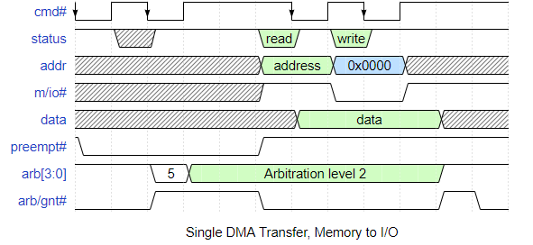
I wish I could say DMA transfers were as simple as there were on ISA, but alas, this is not the case. MCA DMA is, well, tricky.
So let's begin with how a card requests a DMA transfer: the PREEMPT# control line. This is an open-drain line that is shared with all the cards on the bus. To start the DMA transfer, the card just has to pull the PREEMPT# line low (with some caveats on the timing: keep reading).
Once PREEMPT# goes low, the planar decides when to start the arbitration process. The planar needs to do this in case multiple cards assert PREEMPT# at the same time.
First, the planar brings another control line, ARB/GNT# high. When this happens, each card puts its DMA arbitration level (formerly known as the DMA channel number) onto a special 4-bit open-drain arbitration bus, ARB[3:0]. Using combinational logic, each card is supposed to check the state of the bus, starting with the most significant bit. If it is trying to drive a 1 (open-drain means the card lets the pin float) and it reads back a 0, a higher-priority device has won arbitration. At that point the card should give up and not drive the remaining arbitration bus lines. On the other hand, if the bit matches, then the card drives the next bit, checks it, and continues until bit 0. If everything matches, then it wins arbitration and releases the PREEMPT# line. In their hardware interface technical reference manual, IBM provides a schematic for combinational logic that implements this arbitration function. I've redrawn it here using standard logic symbols.
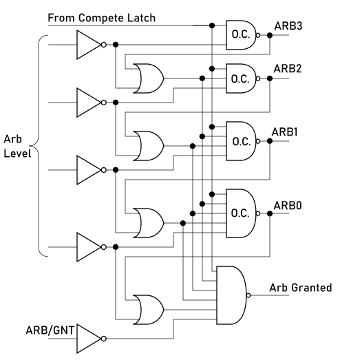
Maybe an example will help. Given two devices, one with a level of 0x2 (0010) and the other with a level of 0x5 (0101):
- Both devices drive bit 3, and both devices notice the value matches what they expect (0).
- Both devices drive bit 2, and the second device (0101) notices a mismatch. It drops out of arbitration and doesn't drive bit 1, which is important.
- The first device drives bit 1, and the value it reads (1) matches what it expects.
- The first device drives bit 0 and notices a match, so it knows that it has won arbitration!
Next, the planar brings ARB/GNT# low, which officially starts the DMA transfer, and the card must release the PREEMPT# immediately. For a single transfer, the DMA controller needs to perform two bus transfers: one to the IO device and one to memory. For read transfers, the IO device gets read first and the result gets written to RAM. For write transfers, RAM is read in the first bus cycle and the IO device gets written to during the second bus cycle. No address is loaded during the IO cycle since it is implied by the DMA priority number.
To end the transfer, the planar pulses ARB/GNT# high and then low again to prepare for the next transfer.
In practice, there are a few wrinkles to look out for. A card should monitor ARB/GNT# and should not request a DMA transfer partway through. The reason is that a late DMA request, occuring in the middle of an arbitration cycle, does not allow enough propagation time for the arbitration logic, and may cause the card to think it has won arbitration when it has actually lost it.
Another wrinkle is that PREEMPT# cannot be asserted during an ongoing DMA cycle unless the status lines S0 and S1 are both high.
In addition, IBM added some "phantom" priority levels that are higher than priority 0, and implemented them in a rather odd way. Priority levels look like the following
| Priority | Purpose |
|---|---|
| -2 | Memory refresh |
| -1 | NMI |
| 0 | DMA channel 0 |
| 1 | DMA channel 1 |
| ... | ... |
| 7 | DMA channel 7 |
| 8 | Available |
| ... | ... |
| E | Available |
| F | System microprocessor |
(Presumably the priority levels marked "Available" can be used by bus masters for regular bus transfers, since that uses the same arbitration mechanism. IBM docs also indicate that DMA channels can be masked off and allocated for use by bus masters.) Notice the negative levels for memory refresh and NMI? Here's how they work:
- PREEMPT# gets asserted by, say, memory refresh.
- PREEMPT# simultaneously gets asserted by some other DMA channel.
- The planar brings ARB/GNT# high, starting an arbitration cycle
- The DMA channel wins arbitration! But wait...
- The planar cheats and leaves ARB/GNT# high, running the bus cycle for memory refresh while the expansion card is waiting for arbitration to end!
- The planar sets ARB/GNT# low, ending arbitration, and then performs the DMA transfer requested by the expansion card.
Conveniently, the DMA IO transfer cycle can be lengthened by the expansion card using the CD_CHRDY signal just like any other synchronous or asynchronous extended cycle.
If an expansion card wants to transfer a block of data at a time, it can request a burst transfer. Remember the arbitration cycle? When the card wins arbitration but before ARB/GNT# goes low, it can pull another control line, BURST#, and hold it low until the last data transfer, at which point it releases the line to let the planar know that no more transfers are needed.
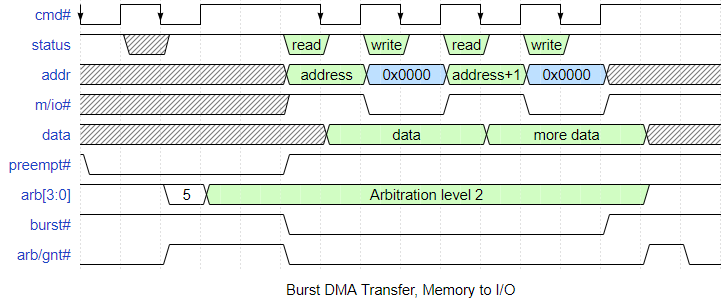
Sounds simple? It's not so bad, but there are caveats.
First, another device can barge in on a burst transfer! Since ARB/GNT# is low during the burst, and only BURST# is continuously held during the transfer (PREEMPT# goes high right after the original device wins arbitration), it is possible for a second device to assert PREEMPT#. When that happens, the first device is supposed to finish the current bus cycle and then release BURST#. Then the planar brings ARB/GNT# high to enter an arbitration cycle. The two devices get to compare DMA priority levels, and the winner can perform a DMA transfer while the loser has to assert PREEMPT# again and wait.
If you think you can cheat by ignoring the other device's PREEMPT# signal and just continue on with your burst transfer, the planar will tolerate this for up to 7.8us before declaring a channel timeout: it drives ARB/GNT# immediately, taking control from the bus master, and then triggers an NMI, which is probably not what you want.
The complexity doesn't end there. Someone at IBM released that certain devices could hog the bus and fill it up with burst transfers, so they added a function called programmable fairness. The concept means that the device whose transfer was paused by the other device requesting DMA is not allowed to participate in that new arbitration cycle! It must wait until the next transfer is done before asserting PREEMPT# and starting a new arbitration cycle. With programmable fairness, two devices attempting burst transfers will share the bus, ping ponging between the two.
Why is the fairness programmable? There's supposed to be a POS register bit that controls it. It defaults to on, however.
Here's a potentially convenient feature. In any transfer involving blocks of data (either bursts or multiple single transfers), the DMA controller maintains a transfer count. When that count reaches zero, the DMA controller on the planar asserts a status line called TC# which lets the expansion card know that the last transfer has occurred. It's totally optional and you can ignore the signal if you don't need it.
So imagine this situation:
- Three expansion cards request burst transfers at the same time. Two have fairness turned on, the other does not.
- In the middle of the transfer, the planar decides to perform a memory refresh
- All the cards are using synchronous extended cycles
- One of the cards is a bus master running with a 225ns cycle time, the DMA controller has a 200ns cycle time, and the CPU has a 187.5ns matched memory bus cycle (see the section below).
- And you wonder why product support for MCA computers was a nightmare!
- Now I have a headache.
This is also the same connector as the VESA Local Bus (VLB). The story goes that IBM was planning on everyone having to use the new bus standard, so the connector companies tooled up and made lots and lots of them. But then the bus didn't really take off outside of IBM, and so the connectors got unloaded for cheap on the open market...
| Pin | Name | Pin | Name |
|---|---|---|---|
| B01 | Audio GND | A01 | CD_SETUP# |
| B02 | Audio | A02 | MADE24 |
| B03 | GND | A03 | GND |
| B04 | 14.318MHZ OSC | A04 | A11 |
| B05 | GND | A05 | A10 |
| B06 | A23 | A06 | A09 |
| B07 | A22 | A07 | +5V |
| B08 | A21 | A08 | A8 |
| B09 | GND | A09 | A7 |
| B10 | A20 | A10 | A6 |
| B11 | A19 | A11 | +5V |
| B12 | A18 | A12 | A5 |
| B13 | GND | A13 | A4 |
| B14 | A17 | A14 | A3 |
| B15 | A16 | A15 | +5V |
| B16 | A15 | A16 | A2 |
| B17 | GND | A17 | A1 |
| B18 | A14 | A18 | A0 |
| B19 | A13 | A19 | +12V |
| B20 | A12 | A20 | ADL# |
| B21 | GND | A21 | PREEMPT# |
| B22 | IRQ9# | A22 | BURST# |
| B23 | IRQ3# | A23 | -12V |
| B24 | IRQ4# | A24 | ARB0 |
| B25 | GND | A25 | ARB1 |
| B26 | IRQ5# | A26 | ARB2 |
| B27 | IRQ6# | A27 | -12V |
| B28 | IRQ7# | A28 | ARB3 |
| B29 | GND | A29 | ARB/GNT# |
| B30 | Reserved | A30 | TC# |
| B31 | Reserved | A31 | +5V |
| B32 | CHCK# | A32 | S0# |
| B33 | GND | A33 | S1# |
| B34 | CMD# | A34 | M/IO# |
| B35 | CHRDYRTN | A35 | +12V |
| B36 | CD_SFD# | A36 | CD_CHRDY |
| B37 | GND | A37 | D0 |
| B38 | D1 | A38 | D2 |
| B39 | D3 | A39 | +5V |
| B40 | D4 | A40 | D5 |
| B41 | GND | A41 | D6 |
| B42 | CHRESET | A42 | D7 |
| B43 | Reserved | A43 | GND |
| B44 | Reserved | A44 | DS_16_RTN# |
| B45 | GND | A45 | REFRESH# |
| B46 | (key) | A46 | (key) |
| B47 | (key) | A47 | (key) |
| B48 | D8 | A48 | +5V |
| B49 | D9 | A49 | D10 |
| B50 | GND | A50 | D11 |
| B51 | D12 | A51 | D13 |
| B52 | D14 | A52 | +12V |
| B53 | D15 | A53 | Reserved |
| B54 | GND | A54 | SBHE# |
| B55 | IRQ10# | A55 | CD_DS_16# |
| B56 | IRQ11# | A56 | +5V |
| B57 | IRQ12# | A57 | IRQ14# |
| B58 | GND | A58 | IRQ15# |
Here's the 32-bit version. It's similar to the 16-bit connector but the rear of the connector has several more pins.
| Pin | Name | Pin | Name |
|---|---|---|---|
| B59 | Reserved | A59 | Reserved |
| B60 | Reserved | A60 | Reserved |
| B61 | Reserved | A61 | GND |
| B62 | Reserved | A62 | Reserved |
| B63 | GND | A63 | Rserved |
| B64 | D16 | A64 | Reserved |
| B65 | D17 | A65 | +12V |
| B66 | D18 | A66 | D19 |
| B67 | GND | A67 | D20 |
| B68 | D22 | A68 | D21 |
| B69 | D23 | A69 | +5V |
| B70 | Reserved | A70 | D24 |
| B71 | GND | A71 | D25 |
| B72 | D27 | A72 | D26 |
| B73 | D28 | A73 | +5V |
| B74 | D29 | A74 | D30 |
| B75 | GND | A75 | D31 |
| B76 | BE0# | A76 | Reserved |
| B77 | BE1# | A77 | +12V |
| B78 | BE2# | A78 | BE3# |
| B79 | GND | A79 | DS_32_RTN# |
| B80 | TR32 | A80 | CD_DS_32 |
| B81 | A24 | A81 | +5V |
| B82 | A25 | A82 | A26 |
| B83 | GND | A83 | A27 |
| B84 | A29 | A84 | A28 |
| B85 | A30 | A85 | +5V |
| B86 | A31 | A86 | Reserved |
| B87 | GND | A87 | Reserved |
| B88 | Reserved | A88 | Reserved |
| B89 | Reserved | A89 | GND |
Each pin has a specific type of driver circuit on the planar. The IBM documentation has a table which can be hard to read, so I've simplified it and included it below.
Drive vs Receive: This refers to the role taken on by this type of expansion card. Should the card drive the signal? Should the card receive the signal?
| Signal | Driver Type | DMA Drive |
DMA Recv |
Memory Drive |
Memory Recv |
IO Drive |
IO Recv |
|---|---|---|---|---|---|---|---|
| A[31:0] | TS | - | R | - | R | - | R |
| D[31:0] | TS | D | R | D | R | D | R |
| ADL# | TS | - | O | - | O | - | O |
| CD_DS_16# | PP | # | - | # | - | # | - |
| DS_16_RTN# | BD | - | - | - | - | - | - |
| SBHE# | TS | - | # | - | # | - | # |
| MADE24 | TS | - | - | - | R | - | - |
| M/IO# | TS | - | R | - | R | - | R |
| S0#, S1# | TS | - | R | - | R | - | R |
| CMD# | TS | - | R | - | R | - | R |
| CD_SFDBK# | PP | D | - | D | - | D | - |
| CD_CHRDY | PP | O | - | O | - | O | - |
| CHRDYRTN | BD | - | - | - | - | - | - |
| ARB[3:0] | OC | D | R | - | - | - | - |
| BURST# | OC | # | - | - | - | - | - |
| PREEMPT# | OC | D | # | - | - | - | - |
| ARB/GNT# | BD | - | R | - | - | - | - |
| TC# | TS | - | O | - | - | - | - |
| IRQn# | OC | O | - | - | - | O | - |
| CD_SETUP# | PP | - | R | - | R | - | R |
| CHCK# | OC | D | - | D | - | D | - |
| REFRESH# | TS | - | O | - | R | - | O |
| OSC | CD | - | O | - | O | - | O |
| CHRESET | BD | - | R | - | R | - | R |
| BE[3:0] | TS | - | R | - | R | - | R |
| CD_DS_32# | PP | # | - | # | - | # | - |
| DS_32_RTN | BD | - | - | - | - | - | - |
| TR_32 | TS | - | - | O | - | O | - |
| Driver Type | Drive/Recv | ||
|---|---|---|---|
| OC | Open Collector | D | Drive enabled |
| TS | Tri-State | R | Receive enabled |
| PP | Push-Pull | O | Optional |
| BD | Bus Driver | - | Not Implemented |
| CD | Clock Driver | # | Required for some implementations |
The MCA bus connector provides a bus reset signal, CHRESET, that the card should use to clear its internal logic. It should also clear the card enable bit in POS register 0x102.
Just like ISA, MCA also provides a 14.318MHz clock signal (4x the NTSC colorburst frequency). Also like ISA, this clock is not necessarily synchronized with the system clock used to generate the rest of the bus signals (like CMD# and ADL#).
Power on MCA is quite nice. There are plenty of ground pins and +5V power pins which really improves signal integrity compared to ISA. There are even +12V and -12V pins for the peripherals that require that.
IBM designed MCA with a method for detecting memory and IO conflicts. Certainly it could do this by checking to see if valid data comes back from a read operation. But how does it know what data is valid? And what about cards that have write-only memory or IO locations? The solution is the card selected feedback line, or CD_SFDBK#.
See, each card is supposed to assert its CD_SFDBK# line whenever it successfully detects an attempt to read and write to any of the memory or IO addresses it decodes to. This is basically the raw output of the address decoder on the card before being latched by CMD# or ADL#. The planar has a giant OR gate so it can tell when any single card has been addressed. A diagnostic program disables all cards but one, and then checks what addresses it responds to, doing this card by card until it figures out the problem.
The card selected feedback line is not used for card setup transfers.
MCA transfers are 8-bit by default. For 16-bit transfers, IBM provides a CD_DS_16# line. If an expansion card supports 16-bit data transfers at specific IO or memory addresses, it asserts CD_DS_16# immediately as it decodes those addresses (not latched by ADL# or CMD#). The planar detects this and sets up the appropriate transfer, enabling the extra data lines.
Things get a little complicated if the PC software is trying to write to the high byte or low byte alone when the target is a 16-bit card. For that, the card has to look at the lowest address bit A0 and another line called SBHE# to figure out the type of transfer:
| A0 | SBHE# | Transfer |
|---|---|---|
| 0 | 1 | Low byte only (D0-D7) |
| 1 | 0 | High byte only (D8-D15) |
| 0 | 0 | Both bytes (D0-D15) |
| 1 | 1 | Invalid |
This is important so the card doesn't inadvertently overwrite the other half of a 16-bit word when handling an 8-bit write.
MCA cards capable of 32-bit transfers have a longer connector edge for more signals. One of the signals is a CD_DS_32# signal which works in a very similar way to the 16-bit version of the signal. The difference is that the data steering is done using a new set of control lines, BE[3:0]. Details are in the technical reference manuals. I won't go into it because if you're really designing a 32-bit card you're really going to want to read the IBM documentation carefully.
Some MCA computers have a slightly longer connector supporting some extra signals that implement the matched memory extension. This allows memory expansion cards installed in such a slot to use a special, short bus cycle called the matched memory cycle (MMC). It's a bizarre feature that behaves differently depending on the computer and even the version of the planar!
You're still curious? OK, the details are pretty nasty. Don't say I didn't warn you.
This transfer only works on 16-bit and 32-bit cards. If the planar can do an MMC, it asserts a line called MMC#. If the card wants to request such an MMC, it asserts an MMCR# line. If the planar chooses to honor the request, instead of asserting ADL# and CMD# in the usual way, it uses a special CMD line called MMC_CMD#.
Oh yeah, it only works this way on the PS/2 Model 80 with a Type 1 planar using a 16MHz 386 CPU. This planar has a default cycle time of 250ns (4 CPU clock cycles of 16MHz), so it is actually slower than my PS/2 Model 50Z's 200ns default cycle (2 CPU cycles of 10MHz). The MMC, on the other hand, manages to shave the transfer time down to 187ns (3 clock cycles). They couldn't use a faster default cycle, most likely, for compatibility with existing cards. So the matched memory extension is a compromise solution that prevents the 16-MHz 386 from having slower RAM access than a 10MHz 286. Hah! I feel sorry for the poor suit-wearing IBM engineers that had to come up with that one.
To make things worse, the matched memory extension only works this way on that exact planar! Later Model 80s with a 20MHz 386 have RAM on the planar tied directly to the CPU and run the MCA bus at a 200ns default cycle, so there's no longer a need for the matched memory extension. The MMC_CMD# line is simply driven low at the same time as the CMD# and the other signals are ignored.
For what it's worth, here is the pinout. These extra pins are added on to the MCA bus connector at the card bracket end. There is no additional key.
| Pin | Name | Pin | Name |
|---|---|---|---|
| BM4 | GND | AM4 | Reserved |
| BM3 | Reserved | AM3 | MMC_CMD# |
| BM2 | MMCR# | AM2 | GND |
| BM1 | Reserved | AM1 | MMC# |
| B01 | ... | A01 | ... |
External memory cards can borrow the planar's RAM refresh signal, REFRESH#. This pulses periodically and the current RAM refresh row can be read from address lines A[8:0] while REFRESH# is asserted.
Many MCA computers have a slightly longer (but with a key separating it from the 16-bit section) connector containing extra signals specific to video cards. These include video sync signals, 8-bit video data, and clock sync lines. This is typical for computers that have VGA graphics built into the planar. The idea is that a video card does not need to support basic VGA video modes or EGA/CGA compatibility and can use this extension to receive raw video from the onboard VGA and pass it through to the card's monitor connector.
The base video extension is even stranger. For PS/2 machines with AVE slots and no VGA on the planar the 32-bit slot is extended to include extra pins so that a video card can provide the AVE signals. The planar just takes these signals and maps them directly to the AVE pins. Yeah, this is technically plug-and-play, but it must have been a real troubleshooting puzzle for someone who didn't know about them.
The AVE pins are separated from the main connector with a keying slot. It's tacked on at the card bracket end.
| Pin | Name | Pin | Name |
|---|---|---|---|
| BV10 | ESYNC | AV10 | VSYNC |
| BV09 | GND | AV09 | HSYNC |
| BV08 | P5 | AV08 | BLANK |
| BV07 | P4 | AV07 | GND |
| BV06 | P3 | AV06 | P6 |
| BV05 | GND | AV05 | EDCLK |
| BV04 | P2 | AV04 | DCLK |
| BV03 | P1 | AV03 | GND |
| BV02 | P0 | AV02 | P7 |
| BV01 | GND | AV01 | EVIDEO |
| (key) | (key) |
Since this is IBM, they offered computers with all sorts of crazy combinations of slot extensions:
- Plain 16-bit slot
- 16-bit slot with AVE
- Plain 32-bit slot
- 32-bit slot with AVE
- 32-bit slot with MME
- 32-bit slot with MME and BVE
MCA has a shared analog audio bus. The manuals call it an audio sum node, but really it is a bidirectional analog voltage signal (typical sum nodes imply a current-based signal transfer). If a card wants to drive sound into the shared bus, it should use an op-amp with a 1.2K resistor in series with the output. If a card wants to receive audio from the bus, it can just run the signal into an op-amp input (the minimum input impedance is 7.5K). Using this approach, sound cards can mix PC speaker noises in with their audio output, or even use the internal PC speaker for audio output. There are two pins for this, AUDIO, and AUDIO GND (a simple-minded approach to avoiding ground loops).
How fast is the MCA bus? Here's a handy table.
| Transfer type | Data rate (MiB/s) |
|---|---|
| MCA 8-bit 200ns | 4.8 |
| MCA 16-bit 200ns | 9.5 |
| MCA 32-bit 200ns | 19.1 |
| MCA 32-bit MMC, 187.5ns | 20.3 |
| MCA 32-bit MMC, 125ns | 30.5 |
| MCA 32-bit streaming, 100ns | 38.1 |
| MCA 64-bit multiplexed streaming, 100ns | 76.3 |
| MCA 64-bit multiplexed streaming, 50ns | 152.6 |
| PCI 32-bit 33MHz | 127.1 |
| PCI 64-bit 33MHz | 254.3 |
| PCI 32-bit 66MHz | 254.3 |
| PCI 64-bit 66MHz | 508.8 |
The 187.5ns MMC is available only on the Model 80 with a Type-1 planar (16MHz 386). Later models typically had memory directly on the planar, tied to the CPU bus directly.
32-bit streaming uses an address auto-increment feature. The address is loaded at the beginning. Every transfer after that is data only and the address is incremented in between automatically.
64-bit streaming cleverly reuses the address bus to transfer 32 additional bits of data (at least, after the initial address is transferred.) The bus is still clocked at only 10MHz.
Some PS/2 devices and expansion cards can support a 50ns bus cycle during streaming mode, and are capable of bus speeds up to 152.6MiB/s, which is slightly faster than 32-bit PCI!
PS/2 Documentation - A collection of scanned PS/2 documentation, including many technical reference manuals.
PS/2 Hardware Interface Technical Reference, First Edition, May 1988 - The primary source for this tutorial.


