Giter Site home page Giter Site logo

yaqwsx / kikit Goto Github PK

View Code? Open in Web Editor NEW
1.4K 34.0 193.0 72.35 MB

Automation tools for KiCAD

Home Page: https://yaqwsx.github.io/KiKit

License: MIT License

Makefile 0.63% Python 95.59% Dockerfile 0.31% HTML 0.30% JavaScript 0.07% CSS 0.14% Shell 2.96%
kicad pcb automation panelization

kikit's Introduction

KiKit – Automation for KiCAD

KiKit Logo

KiKit is a Python library, KiCAD plugin and a CLI tool to automate several tasks in a standard KiCAD workflow like:
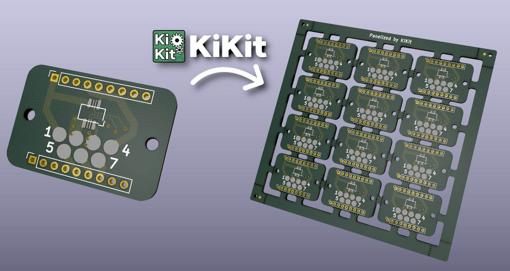
KiKit Promo

Do You Enjoy KiKit or Does It Save You Time?

Then definitely consider:

Your support will allow me to allocate time to properly maintain my projects like this.

PS: Be sure to check out my other KiCAD & PCB related projects:

Installation

KiKit is available as a PyPi package. However, due to packaging of KiCAD, installation on some platforms requires usage of specific Python interpreter.

Please follow the detailed installation guide that covers installation based on the platform you use.

Why Should I Use It?

Everything KiKit does, can also be done via Pcbnew in KiCAD. However, you have to do it manually. One of the common scenarios is the creation of panels. Most of the tutorials on the internet guide you to use the "append board" functionality of Pcbnew. However, this approach is labour-intensive, error-prone and whenever, you change the board, you have to do it again.

With KiKit you just call a CLI command if you have a simple layout (e.g., a grid) or write few Python instructions like "place board here", "add bridge here", "separate boards via mouse bites/v-cuts" and you are done. The process is repeatable and actually much simpler than hand-drawing the panels. KiKit also allows you to easily export all the Gerbers in a single step.

You can then write a Makefile and simply call make to get all your manufacturing data and board presentation pages.

Feature List

How To Use It?

Start with reading the panelization documentation. This page will you guide through CLI, GUI and scripting usage. Also don't miss the examples. There is also a quick not on how to use panelization action plugin. If you are interested in generating solder paste stencils, see Stencil documentation

Acknowledgements

The project is supported by:

KiKit Is Broken or Does Not Work as Expected

Please, first check FAQ. If you have not found answer for your problem there, feel free to open an issue on GitHub.

If you would like to have a feature in KiKit that is currently not on a roadmap, or if you need to prepare custom panelization script (e.g., multi-design panels, panels with specific arrangement), you can consider hiring me to do the job. Just reach out to me via e-mail and we can discuss further details.

kikit's People

Contributors

a7hybnj2 avatar chatelao avatar conradopoole avatar cubesky avatar dependabot[bot] avatar eddwhite avatar errno avatar gmarull avatar j4m3s avatar jbower-fb avatar kliment avatar leo60228 avatar lukasz-skalski avatar mairas avatar maribu avatar markh-de avatar mayl avatar mplacona avatar pancelka avatar pekkaroi avatar putyn avatar romavis avatar sebastiangrau avatar set-soft avatar smittyhalibut avatar troky avatar tywtyw2002 avatar vagnum08 avatar vipqualitypost avatar yaqwsx avatar

Stargazers

 avatar  avatar  avatar  avatar  avatar  avatar  avatar  avatar  avatar  avatar  avatar  avatar  avatar  avatar  avatar  avatar  avatar  avatar  avatar  avatar  avatar  avatar  avatar  avatar  avatar  avatar  avatar  avatar  avatar  avatar  avatar  avatar  avatar  avatar  avatar  avatar  avatar  avatar  avatar  avatar  avatar  avatar  avatar  avatar  avatar  avatar  avatar  avatar  avatar  avatar  avatar  avatar  avatar  avatar  avatar  avatar  avatar  avatar  avatar  avatar  avatar  avatar  avatar  avatar  avatar  avatar  avatar  avatar  avatar  avatar  avatar  avatar  avatar  avatar  avatar  avatar  avatar  avatar  avatar  avatar  avatar  avatar  avatar  avatar  avatar  avatar  avatar  avatar  avatar  avatar  avatar  avatar  avatar  avatar  avatar  avatar  avatar  avatar  avatar  avatar

Watchers

 avatar  avatar  avatar  avatar  avatar  avatar  avatar  avatar  avatar  avatar  avatar  avatar  avatar  avatar  avatar  avatar  avatar  avatar  avatar  avatar  avatar  avatar  avatar  avatar  avatar  avatar  avatar  avatar  avatar  avatar  avatar  avatar  avatar  avatar

kikit's Issues

KiKit does not inherit layer count

When panelizing a 4 layer board, I discovered that KiKit generates a panel with only 2 layers. If a user does not notice this and manually enable any inner layers they will not get a working panel.

Generate tabs based on line segments in given layer

Allow the user to draw lines e.g. in the Eco1.User layer, which will be treated as tab origins and directions. This will make it easy for custom tab placement. Allow the user to use it from CLI - specify either --tabwidth + --tabheight + --htabs + --vtabs or --tabslayer + --tabwidth.

Idea - is there a way user can specify width of individual tabs in KiCAD?

ModuleNotFoundError: No module named 'pcbnew'

Hello,

I tried kikit on Ubuntu 18.04 and MacOs. I installed it one time from the repository with python3 install and one time from pip3. In both cases and with several kicad_pcb files I get the following error message. Is there a pcbnew package I have install?

Best Christian

/usr/local/bin/kikit panelize grid --space 2 --gridsize 2 2 --tabwidth 3 --tabheight 3 --mousebites 0.5 1 0.25 --radius 1 --panelsize 80 80 /tmp/test.kicad_pcb /tmp/panel.kicad_pcb
Traceback (most recent call last):
  File "/usr/local/bin/kikit", line 11, in <module>
    load_entry_point('KiKit==0.3', 'console_scripts', 'kikit')()
  File "/home/user/.local/lib/python3.6/site-packages/pkg_resources/__init__.py", line 490, in load_entry_point
    return get_distribution(dist).load_entry_point(group, name)
  File "/home/user/.local/lib/python3.6/site-packages/pkg_resources/__init__.py", line 2854, in load_entry_point
    return ep.load()
  File "/home/user/.local/lib/python3.6/site-packages/pkg_resources/__init__.py", line 2445, in load
    return self.resolve()
  File "/home/user/.local/lib/python3.6/site-packages/pkg_resources/__init__.py", line 2451, in resolve
    module = __import__(self.module_name, fromlist=['__name__'], level=0)
  File "/usr/local/lib/python3.6/dist-packages/KiKit-0.3-py3.6.egg/kikit/ui.py", line 2, in <module>
    import kikit.export as kiexport
  File "/usr/local/lib/python3.6/dist-packages/KiKit-0.3-py3.6.egg/kikit/export.py", line 5, in <module>
    from pcbnew import *
ModuleNotFoundError: No module named 'pcbnew'

Mousebites issues?

You don't specify a default here, so maybe this is just a documentation issue.

I've made boards where I have traces right up against the edge of the board. A positive offset on the mousebites might be problematic as that could cut into traces.

So in your example --mousebites 0.5 1 0.25 produces this.
image

If offset is negative, the mousebites move off the board and back into the tab.

I was thinking the default offset for mousebites would be 1/2 the radius of the mousebites so the edge of the mousebites would be the normal edge of the board.

Version command

Hi,

OS:- Ubuntu 20.04

Can we add command to check kikit version?
I just got notification that v0.6.0 is released so I am trying to update in on my machine but I am not sure if I get latest release installed or not.
If we can add add -version command then we can always make sure that we are on latest release or not.

Problem panelizing circular board

When trying to panelize the board available in this github repository: https://github.com/EnJens/ilulissat (a fully circular board),

I'm using a trivial script based on the example for initial testing:

from kikit.panelize import Panel, fromMm
from pcbnew import *
panel = Panel()
size, cuts = panel.makeGrid("ilulissat.kicad_pcb", 4, 3, wxPointMM(100, 40),
            tolerance=fromMm(5), verSpace=fromMm(5), horSpace=fromMm(5),
            outerHorTabThickness=fromMm(3), outerVerTabThickness=fromMm(3),
            verTabWidth=fromMm(15), horTabWidth=fromMm(8),
            radius=fromMm(1))
panel.makeMouseBites(cuts, diameter=fromMm(0.5), spacing=fromMm(1))
panel.makeFrame(size, fromMm(100), fromMm(100), fromMm(3), radius=fromMm(1))
panel.save("panel.kicad_pcb")

Running the script I get the error:

Traceback (most recent call last):
  File "panelize.py", line 4, in <module>
    size, cuts = panel.makeGrid("ilulissat.kicad_pcb", 4, 3, wxPointMM(100, 40),
  File "kikit/panelize.py", line 553, in makeGrid
    cuts = self._makeSingleInnerTabs(gridDest, rows, cols, boardSize,
  File "kikit/panelize.py", line 473, in _makeSingleInnerTabs
    self.appendSubstrate(tab, radius)
  File "kikit/panelize.py", line 313, in appendSubstrate
    for geom in filletCandidates:
TypeError: 'LineString' object is not iterable

Specify path of pcbnew

So this is kinda related to #21
I'm using two different versions of KiCAD: The latest stable release from my distribution (ie 5.1.6-1) and a custom self-compiled version which is used in my company.
I'm doing this because we quite like some of the newly introduced features but still want to edit and distribute schematics with the stable release for use by other people.
Now when I want to panelize newer boards I'm greeted with this error:

An error occurred: KiCad was unable to open this file, as it was created with
a more recent version than the one you are running.
To open it, you'll need  to upgrade KiCad to a more recent version.

Date of KiCad version required (or newer): 09/07/19

Full error text:
Unexpected "max_error" in input/source
"test-board.kicad_pcb"
line 50, offset 6
No output files produced

That's the same error I get when I try opening newer kicad_pcb-files with an older version of pcbnew. They are incompatible because of some added options, max_error is just one of these.

Now I can kinda circumvent this by just deleting the offending options from the raw file but it would be nicer if I could specify the pcbnew-binary used by KiKit.

I know, that's quite a niche error case, but this tool has been proven to be invaluable and I'd like it to be just a tad more awesome :)

missing packages on panelized board

Hi !

I just noticed i've got some missing packages on my panelized board using pip package, and on current master.

Screenshot from 2020-04-28 19-07-29
Screenshot from 2020-04-28 19-07-41

Is there a way to get some error / verbose traces ? Are you interested by the pcb file ?

Thanks for the awesome tool !

Panel does not include outside edge vcuts when --space set to 0

Describe the bug:
When running panelize command with --vcuts and --space 0 the output panel does not include vcuts on the outside edge of the boards in the panel. See images in steps to reproduce

Expected behavior:
I expected vcuts to always be added to the outside edge.

To Reproduce

Run a panelize command like this:
kikit panelize grid --space 1 --gridsize 2 2 --vcuts --panelsize 100 100 ...

Notice the vcuts on the outside edge of the board are included (marked with red arrows)
image

Now run the same command with --space 0
Run a panelize command like this:
kikit panelize grid --space 0 --gridsize 2 2 --vcuts --panelsize 100 100 ...

Notice the outside edge vcuts are missing:
image

A LinearRing must have at least 3 coordinate tuples

Describe the bug:

$ kikit panelize grid --gridsize 2 3  decade.kicad_pcb decade_panel.kicad_pcb

An error occurred: A LinearRing must have at least 3 coordinate tuples
No output files produced

Expected behavior: A clear and concise description of what you expected to happen.

A panel to have been made using the defaults for a 2x3 grid.

To Reproduce

Create a panel with a 2x3 grid with the following board.

https://github.com/rcludwick/decade-box

Source board:

https://github.com/rcludwick/decade-box

KiKit command:

$ kikit panelize grid --gridsize 2 3  decade.kicad_pcb decade_panel.kicad_pcb

Version

0.6.0/master.

Error is hidden behind #66.

Tightgrid not producing proper mouse bites.

When using tightgrid and mousebites, some slots on the edges don't form properly.

the command I am running is:

kikit panelize tightgrid --gridsize 6 4 --mousebites 0.5 1 -0.25 --radius 1 --htabs 1 --vtabs 1 --panelsize 100 100 --slotwidth 2.0 --tabwidth 3 --tabheight 3 --space 3.3 ../AP3211-v2.0.kicad_pcb ap3211-panel.kicad_pcb

I have attached the input and output files as a .zip (github doesn't accept kicad_pcb.
panelbug.zip

KiKit panel does not inherit design rules.

Noticed that the panel generated by KiKit does not inherit the design rules from the design being panelized. This makes it so you cannot run a successful DRC on the panel. I think it would be nice to have the panel inherit the design rules of the individual board so that you can do a nice, final sanity DRC check on the panel before submitting for fab (would even be cool if KiKit could do that from the command line....).

Sorry for the flurry of issues/pull requests all at once, obviously I've been using KiKit the past few days and I feel like it's better to track these things as I come across them!

Add cuts to the panel frame

There should be cuts on the panel frame to make it easy to break:

instructions

This is missing for mouse bites.

There are two ways to implement; either:

  • that makeGrid will also build the frame and it will not be an independent step (makeGrid and then makeFrame) or
  • makeFrame has to take boardsize and spacing to make the cuts. Therefore, makeGrid has to return it.

It could be possible to introduce PanelInfo - structure gradually filled by panel operations, however, it yields tight coupling between the individual functions, which is rather undesirable.

Error during open kikit on Raspberry Pi 4 Debian Buster

Installation of kikit completed successfuly. Before I did sudo apt-get update & upgrade
Once try to run kikit I get error

OSError: Could not find lib geos_c or load any of its variants ['libgeos_c.so.1', 'libgeos_c.so']

tried re-install shapely and geos without success.
Only using : sudo apt-get install libgeos-dev
I've managed to fix issue and run the kikit.

Version

  • the output of kikit --version
    KiKit (0.5.3) - Automation for KiCAD boards
    INSTALLED: 0.5.3 (latest)

  • source of installation (PyPI or upstream version)
    PyPI

  • your operating system Raspbery Pi 4 2GB Raspian Buster

An error occurred: Discontinuous outline

I am new with pcb things, I just want panellise a small opensource pcb (link below) but i face problem :

An error occurred: asset/the_pcb.kicad_pcb: Discontinuous outline at [251.419999, 105.989999]

error message sounds there some thing wrong the kicad file but i have no idea what it means and I did not found any documentation about it.

but when i run with your example , conn.kicad_pcb, everything run perfectly.

To Reproduce

Source board: https://drive.google.com/file/d/1QVeXxAqZElhmPN7tkkNfsAEIB8NRFTR0/view?usp=sharing
KiKit command:

kikit panelize grid --gridsize 2 2 --vcuts asset/the_pcb.kicad_pcb asset/the_pcb_panel.kicad_pcb

Version

Specify which version of KiKit do I use:

  • the output of kikit --version
kikit, version 0.6.1```
- run on docker from given dockerfile

Feature request: Corner joints

Would be great if there was an option in addition to Vcuts and mouse bites, to have the diagonal tabs in the corners.

Add support for rails

Currently, KiKit can generate only frames. It would be nice if it could also produce rails as requested in #40:

image

An error occurred: No intersection found within given distance. No output files produced

Describe the bug:
Recieve the error: "An error occurred: No intersection found within given distance. No output files produced"

Expected behavior: Panelized board with vcuts

Be Gentle with me please. I'm very new to using this so it's entirely likely I've just messed up the command somehow.
I realize there would be very few boards on this panel given the size of the panel and the size of the board.
I'm re-using a command from a previous successful run to try and minimize errors.

I'm trying to get vertical v-cuts on the short ends with some tabs separating the boards, and horizontal v-cuts on the long edges with some tabs separating the boards.

could the issue be that there is a narrower section of the board where the sensor elements are placed?

To Reproduce

Source board: https://github.com/Kd5ahl/BME-BH1750/blob/master/BME%20Lux%20Sensor-BH1750.kicad_pcb

KiKit command: kikit panelize grid --space 3 --gridsize 3 2 --tabwidth 25 --tabheight 25 --vcuts --radius 1 --panelsize 100 100 BME\ Lux\ Sensor-BH1750.kicad_pcb BME\ Lux\ Sensor-BH1750-Panel.kicad_pcb

Screenshots

If applicable, add screenshots to help explain your problem.

Version

**> kikit --version

Usage: kikit [OPTIONS] COMMAND [ARGS]...
Try 'kikit --help' for help.

Error: no such option: --version
It's fairly recent though, installed it within the last couple of weeks.**

  • source of installation (PyPI or upstream version)

> PyPI

  • your operating system
    > Ubuntu 20.04

[RFC] Add copper fill

Specially for FPC panels it is desirable to fill all the unused areas with copper. The rationale in that case is twofold. in one hand it reduces the amount of etching, on the other it produces a significantly sturdier panel for further processing.

This could be done by simply stretching a lowest priority copper zone over the entire area of the PCB and filling only that zone. I have tried this manually on the finished panel PCB and it has worked.

One issue though is that PCBNEW does not allow zone priorities lower than 0. There are two ways to work that around. One is to require the user to have all their zones with priority >=1 when using this feature; the other is to automatically bump the priority of all the zones by one (I have no idea how to do this in the Python API)

KiKit should be able to export a bom and pos file

I really like how KiKit allows a pcb processing pipeline to be created where a design can be automatically panelized, and gerbers exported for fabrication. To make this process complete, I think there should also be options for generating a bom and pick and place position file. This way an entire fabrication and assembly package for a design could be generated without any manual intervention. Is there interest in such a feature?

Docs issue

I have just found this fantastic (at least in theory) project and trying to play with it but I get mixed results.

kikit panelize grid --space 3 --gridsize 2 2 --tabwidth 3 --tabheight 3 --htabs 1 --vtabs 2 --mousebites 0.5 1 0.25 --radius 1

gives me

Usage: kikit panelize grid [OPTIONS] INPUT OUTPUT
Try "kikit panelize grid --help" for help.

Error: no such option: --htabs

So I did check that those options are gone but after giving INPUT and OUTPUT I get:

Usage: kikit panelize grid [OPTIONS] INPUT OUTPUT
Try "kikit panelize grid --help" for help.

Error: Got unexpected extra argument (panel.kicad_pcb)

KiKit does not port over the board thickness to the panel

Related to issue #36 is that the PCB substrate thickness is not ported over either. That is important for mechanical outputs (STEP/FcSTD) of the board when the board is not 1.6mm thick. Optionally if appending more than one board it could be a good check to add a warning/error if a board is imported with a thickness different to the panel. (If not explicitly set it should take the thickness of the first board appended).

Left and right rail V-cut missing

Describe the bug: Left and right rail V-cut missing

Expected behavior: V-Cut between left/right rails and boards

Panelize a board using

kikit panelize grid --space 0 --gridsize 4 2 --vcuts --railsLr 10 --tooling 5 5 3 <...> `

Source board: N/A
KiKit command:

kikit panelize grid --space 0 --gridsize 4 2 --vcuts --railsLr 10 --tooling 5 5 3 <...> `

Screenshots

If applicable, add screenshots to help explain your problem.
image

Version:

v0.6.0 via latest docker image

Option to change annotations on panelized boards

Would it be possible to add an option to change the annotations on the panelized boards? Similar to what KiKit is doing with net names already. For example: D1->Board_1-D1.
I would like to create CPL file for the panelized boards so I can get boards made and assembled at one go at JLCPCB...

Wrong X/Y when extracting a board -> misleading error

Hi,

THX for this nice tool!

When extracting a board and you don't give the correct corner for extracting, you will get following error:
An error occurred: ../breakout.kicad_pcb: Discontinuous outline at [X,Y]

Please clarify in the example that the upper left corner is necessary for extracting the board.

Greetings

Missing component and mountingholes in output file

I have made a pcb 30x50mm, that I panelized with this command:
kikit panelize grid --space 3 --gridsize 2 5 --tabwidth 3 --tabheight 3 --htabs 1 --vtabs 1 --mousebites 0.5 1 0.25 --radius 1 --panelsize 180 120 v4.kicad_pcb panel.kicad_pcb

In the output file one component and all 4 mounting holes in the corners are missing, is there a way i can debug this ?

Implement a `Cut` class to make cuts more powerful

It would be nice to implement a Cut class to represent a board cut. Currently, we use only a pair of points - therefore a cut is a line segment. However, it does not preserve the orientation of the cut - the direction to the board and out of the board. It could be implemented even with a tuple, but it has no clear interface to communicate the orientation, therefore, it is error-prone.

The cut orientation is useful e.g. for mouse bites - they should not lie directly in the cut line but should be moved by 0.25 mm into the board. Also, when we introduce a Cut class, we can easily implement arc cuts (if it is desirable)

Create a Panel with multiple different design

Hi,
I have been using Gerbertools to create a panel design and recently I found that I am not able to generate 4mm longer tab routing tabs and factory was saying no for the panels. And then I found Kikit and it fixed this problem as now I can make any customize in length that factory supports.

So for single design panel kikit is doing great job. Thank you yaqwsx for this.
Do we have any option to merge multiple different design and have a panel designed for that?

Feature request - Tooling holes and Fiducial marks

When creating a panel where there is an tooling area along the edge, it would be really useful to be have the option to add tooling holes and fiducial marks.

It would be great if there was a sensible default for the tooling holes of 3.2mm 5mm from the corner of the panel, and for the fiducial 5mm from the horizontal edge, and 10mm from the vertical edge, (to put them 5mm to the side of the tooling holes).

Thanks

Problems with CLI

Hello. I type this:

$ kikit panelize grid --gridsize 2 2 ./atmega328pb.kicad_pcb ./grb/test.grbl

I see this:

Traceback (most recent call last):
  File "/home/denis/.local/bin/kikit", line 11, in <module>
    sys.exit(cli())
  File "/home/denis/.local/lib/python3.6/site-packages/click/core.py", line 829, in __call__
    return self.main(*args, **kwargs)
  File "/home/denis/.local/lib/python3.6/site-packages/click/core.py", line 782, in main
    rv = self.invoke(ctx)
  File "/home/denis/.local/lib/python3.6/site-packages/click/core.py", line 1259, in invoke
    return _process_result(sub_ctx.command.invoke(sub_ctx))
  File "/home/denis/.local/lib/python3.6/site-packages/click/core.py", line 1259, in invoke
    return _process_result(sub_ctx.command.invoke(sub_ctx))
  File "/home/denis/.local/lib/python3.6/site-packages/click/core.py", line 1066, in invoke
    return ctx.invoke(self.callback, **ctx.params)
  File "/home/denis/.local/lib/python3.6/site-packages/click/core.py", line 610, in invoke
    return callback(*args, **kwargs)
  File "/home/denis/.local/lib/python3.6/site-packages/kikit/ui.py", line 69, in grid
    outerHorTabThickness=oht, outerVerTabThickness=ovt)
  File "/home/denis/.local/lib/python3.6/site-packages/kikit/panelize.py", line 551, in makeGrid
    sourceArea, tolerance, verSpace, horSpace)
  File "/home/denis/.local/lib/python3.6/site-packages/kikit/panelize.py", line 414, in _placeBoardsInGrid
    dest = self._boardGridPos(destination, i, j, boardSize, horSpace, verSpace)
  File "/home/denis/.local/lib/python3.6/site-packages/kikit/panelize.py", line 402, in _boardGridPos                                                            
    return wxPoint(destination[0] + j * (boardSize.GetWidth() + horSpace - FromMM(0.001)),                                                                       
TypeError: unsupported operand type(s) for +: 'int' and 'NoneType' 

If I type this:

$ kikit panelize grid --gridsize <2 2> ./atmega328pb.kicad_pcb ./grb/test.grbl
I get this:

bash: 2: Adresář nebo soubor neexistuje

So, what nextz..?

More than one mousebite?

With the pip code I see --htabs and --vtabs are gone? I'm getting just one mousebite? Not enough for 7cm edge.

Segmentation fault (core dumped)

I used to work with kikit few months ago and everything was fine. Until today. This is the command which I used before:

kikit panelize grid --space 2 --gridsize 1 5 --tabwidth 5 --tabheight 5 --mousebites 0.5 1 0 --htabs 3 --vtabs 2 --radius 0.8 ../evse.kicad_pcb evse_5x.kicad_pcb

Today I wanted to experiment with custom mousebite position and it just did not work, so I upgraded kikit. I tried 0.5, 0.6.0 and 0.6.1 (pip3 install 'kikit==0.6.1') and now I am only receiving "segmentation fault (core dumped)" after running the script...

Python 3.6.9
Xubuntu 18.04
KiCAD 5.1.6

What can be wrong? some problem in local python installation or kikit? I tried to modify the script parameters, also different PCB, no success...

Radius error

I am having trouble using this tool with a specific board and I don't understand the error it is throwing:

An error occurred: Cannot make smaller radius than 0.01 mm
No output files produced

Expected behavior:
PCB panel would be generated

To Reproduce

PCB layout that triggers this:
https://github.com/Chameleon-Electronics/programmer-adapter/releases/tag/v1.3.0 (PCB attached)

Source board: <include your .kicad_pcb file here>
KiKit command:

kikit panelize grid --gridsize 2 2 --vcuts programmer-adapter.kicad_pcb panel.kicad_pcb

Screenshots

Not applicable

Version

0.5.2

Reconstruct arcs in Edge.Cuts

Current implementation removes arcs and circles in the internal representation of a substrate and approximates them with lines (mimicking what Shapely does). It would be nice to reconstruct arcs when exporting the board.

The challenges are:

  • we can test if consequential points lie on the same circle, however, then we may deduce false arcs - e.g. if the input board was a regular polygon
  • we can store a list of original arcs and match them back - however, parts of the arcs might be lost during substrate merging

Corner fillets not generated for frames.

This can be seen even in the documentation for the panelization feature:
image

The inner corners of the frame and where the tabs meet the frame are not radius like the rest of the board.

Shadowing import in line 340 of panelize.py

Describe the bug: A clear and concise description of what the bug is.

Looking at the following code, the variable substrate shadows the "import substrate" above.

Line 340 of panelize.py:

        try:
            substrate = Substrate(edges, bufferOutline)
            self.boardSubstrate.union(substrate)
            self.substrates.append(substrate)
        except substrate.PositionError as e:
            point = undoTransformation(e.point, rotationAngle, originPoint, translation)
            raise substrate.PositionError(filename + ": " + e.origMessage, point)

Once substrate is defined, that causes a namespace conflict with the except statement as substrate points to an instance of the class Substrate() not the package named substrate.

Version

Master branch

Fiducial Point is getting removed

I do have 4 Fiducial points in design two on top side and two on bottom.
After applying command to create a grid 2x1 with tabs. I see there is only one fiducial that on bottom side is there other three goes away in penalized PCB.

Internal routed shapes disappear in panelized board

So I just discovered KiKit, and after figuring out how to get it installed, I've been quite pleased with how well it handles an otherwise tedious process.
However, I have an issue. My pre-panelized PCB (60x20mm) has a few routed slots on the PCB (which I placed on Edge.Cuts). But after panelization with KiKit, however, these routed slots are missing.

I'm not really complaining, as it's way easier to re-add the routed slots, than panelize by hand. Except that copy-paste between instances in KiCad has been broken again, so...

Recommend Projects

  • React photo React

    A declarative, efficient, and flexible JavaScript library for building user interfaces.

  • Vue.js photo Vue.js

    🖖 Vue.js is a progressive, incrementally-adoptable JavaScript framework for building UI on the web.

  • Typescript photo Typescript

    TypeScript is a superset of JavaScript that compiles to clean JavaScript output.

  • TensorFlow photo TensorFlow

    An Open Source Machine Learning Framework for Everyone

  • Django photo Django

    The Web framework for perfectionists with deadlines.

  • D3 photo D3

    Bring data to life with SVG, Canvas and HTML. 📊📈🎉

Recommend Topics

  • javascript

    JavaScript (JS) is a lightweight interpreted programming language with first-class functions.

  • web

    Some thing interesting about web. New door for the world.

  • server

    A server is a program made to process requests and deliver data to clients.

  • Machine learning

    Machine learning is a way of modeling and interpreting data that allows a piece of software to respond intelligently.

  • Game

    Some thing interesting about game, make everyone happy.

Recommend Org

  • Facebook photo Facebook

    We are working to build community through open source technology. NB: members must have two-factor auth.

  • Microsoft photo Microsoft

    Open source projects and samples from Microsoft.

  • Google photo Google

    Google ❤️ Open Source for everyone.

  • D3 photo D3

    Data-Driven Documents codes.