This is an open source PSRAM/HyperRAM controller for the Tang Nano 9K FPGA board. The chip is Gowin GW1NR-LV9QN88PC6/15.
Overview
- Supports both word (16-bit) and byte based access. No bursting is used.
- 1:1 clock design. Memory and main logic work under the same clock. Max clock frequency is 83Mhz.
- I'm mostly aiming for low access latency. Write latency is 7 cycles (1x) or 10 cycles (2x). Read latency is 12 cycles (1x) or 15 cycles(2x). HyperRAM needs 2x latency now and then for automatic DRAM refreshes. In my test, 2x latency happens about 0.05% of time.
- Uses Gowin's ODDR/IDDR primitives. This removes the need to use double frequency clocks. A PLL is used to generate the phase-shifted clock needed by HyperRAM.
- Code is simple. 200 lines of Verilog. Resource usage: <200 logic units, vs ~1000 for official IP.
Usage
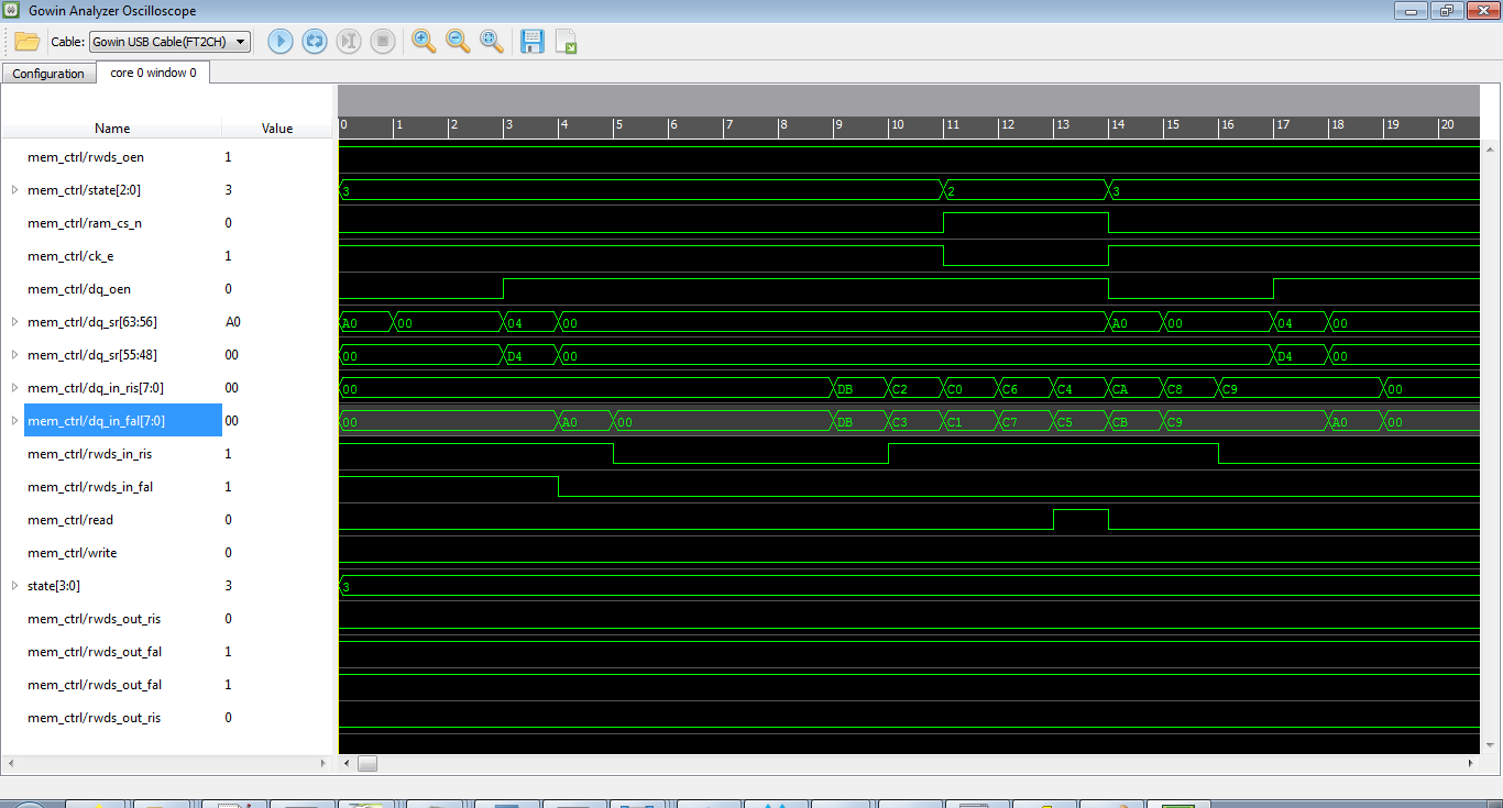
psram_controller.vis the controller. See comments for usage.- Also read the test bench
psram_test_top.vfor an actual example. It works at 81 Mhz, uses byte-based access, and writes its results to UART at 115200 bps.
Quick discussion about going above 83Mhz
- The LATENCY parameter specifies the tACC (initial latency) cycles. Setting it to 4 to 6 allows higher frequency on the RAM side. However currently this does not work due to failing to achieve timing closure on the FPGA side. This is probably due to the speed grade of the chip as similar code works at higher frequencies on Tang Primer 20K (with C8/17 speed grade). I conjecture this to be the reason why the official PSRAM HS IP uses a 1:2 gear ratio design. Eseentially that controller runs at half the memmory clock speed. You can confirms this by building the official IP and check its resource usage. In my case it uses 1 CLKDIV, 16 IDES4 and 23 OSER4, but no IDDR/ODDR. So for memory speed of 160Mhz, the controller is running at 80Mhz (thus the CLKDIV) and sending/receiving 4 bits every cycle on one signal line (IDES4/OSER4). So one could adopt a similar approach to achieve higher memory speed. This GW2A DDR3 controller using ISER8/OSER8 primitives may be of value if anyone is interested in implementing such a HyperRAM controller.
See also
- An example using the official Gowin HyperRAM IP. The official IP uses bursting access (writes/reads >= 16 bytes a time). So it is higher throughput, but also higher latency. And it is encrypted verilog. :(
- Tang 20K official examples, where the UART module comes from.
Feng Zhou, 2022.8