Opensource RISC-V implemented from scratch in one night!
- DarkRISCV
Developed in a magic night of 19 Aug, 2018 between 2am and 8am, the DarkRISCV softcore started as an proof of concept for the opensource RISC-V instruction set.
Although the code is small and crude when compared with other RISC-V implementations, the DarkRISCV has lots of impressive features:
- implements most of the RISC-V RV32E instruction set
- implements most of the RISC-V RV32I instruction set (missing csr*, e* and fence*)
- works up to 250MHz in a ultrascale ku040 (400MHz w/ overclock!)
- up to 100MHz in a cheap spartan-6, fits in small spartan-3E such as XC3S100E!
- can sustain 1 clock per instruction most of time (typically 71% of time)
- flexible harvard architecture (easy to integrate a cache controller, bus bridges, etc)
- works fine in a real xilinx (spartan-3, spartan-6, spartan-7, artix-7, kintex-7 and kintex ultrascale)
- works fine with some real altera and lattice FPGAs
- works fine with gcc 9.0.0 for RISC-V (no patches required!)
- uses between 850-1500LUTs (core only with LUT6 technology, depending of enabled features and optimizations)
- optional RV32E support (works better with LUT4 FPGAs)
- optional 16x16-bit MAC instruction (for digital signal processing)
- optional coarse-grained multi-threading (MT)
- no interlock between pipeline stages!
- BSD license: can be used anywhere with no restrictions!
Some extra features are planned for the future or under development:
- interrupt controller (under tests)
- cache controller (under tests)
- gpio and timer (under tests)
- sdram controller w/ data scrambler
- branch predictor (under tests)
- ethernet controller (GbE)
- multi-processing (SMP)
- network on chip (NoC)
- rv64i support (not so easy as it appears...)
- dynamic bus sizing and big-endian support
- user/supervisor modes
- debug support
- misaligned memory access
- bridge for 8/16/32-bit buses
And much other features!
Feel free to make suggestions and good hacking! o/
The initial concept was based in my other early 16-bit RISC processors and composed by a simplified two stage pipeline, where a instruction is fetch from a instruction memory in the first clock and then the instruction is decoded/executed in the second clock. The pipeline is overlapped without interlocks, in a way that the DarkRISCV can reach the performance of one clock per instruction most of time, except by a taken branch, where one clock is lost in the pipeline flush. Of course, in order to perform read operations in blockrams in a single clock, a single-phase clock with combinational memory OR a two-phase clock with blockram memory is required, in a way that no wait states are required in thatcases.
As result, the code is very compact, with around three hundred lines of obfuscated but beautiful Verilog code. After lots of exciting sleepless nights of work and the help of lots of colleagues, the DarkRISCV reached a very good quality result, in a way that the code compiled by the standard GCC for RV32I worked fine.
After two years of development, a three stage pipeline working with a single clock phase is also available, resulting in a better distribution between the decode and execute stages. In this case the instruction is fetch in the first clock from a blockram, decoded in the second clock and executed in the third clock.
As long the load instruction cannot load the data from a blockram in a single clock, the external logic inserts one extra clock in IO operations. Also, there are two extra clocks in order to flush the pipeline in the case of taken branches. The impact of the pipeline flush depends of the compiler optimizations, but according to the lastest measurements, the 3-stage pipeline version can reach a instruction per clock (IPC) of 0.7, smaller than the measured IPC of 0.85 in the case of the 2-stage pipeline version.
Anyway, with the 3-stage pipeline and some other expensive optimizations, the DarkRISCV can reach up to 100MHz in a low-cost Spartan-6, which results in more performance when compared with the 2-stage pipeline version (typically 50MHz).
The main motivation for the DarkRISCV was create a migration path for some projects around the 680x0/Coldfire family.
Although there are lots of 680x0 cores available, they are designed around different concepts and requirements, in a way that I found no much options regarding my requirements (more than 50MIPS with around 1000LUTs). The best option at this moment, the TG68, requires at least 2400LUTs (by removing the MUL/DIV instructions), and works up to 40MHz in a Spartan-6. As addition, the TG68 core requires at least 2 clock per instruction, which means a peak performance of 20MIPS. As long the 680x0 instruction is too complex, this result is really not bad at all and, at this moment, probably the best opensource option to replace the 68000.
Anyway, it does not match with the my requirements regarding space and performance. As part of the investigation, I tested other cores, but I found no much options as good as the TG68 and I even started design a risclized-68000 core, in order to try find a solution.
Unfortunately, due to compiler requirements (standard GCC), I found no much ways to reduce the space and increase the performance, in a way that I started investigate about non-680x0 cores.
After lots of tests with different cores, I found the picorv32 core and the all the ecosystem around the RISC-V. The picorv32 is a very nice project and can peak up to 150MHz in a low-cost Spartan-6. Although most instructions requires 3 or 4 clocks per instruction, the picorv32 resembles the 68020 in some ways, but running at 150MHz and providing a peak performance of 50MIPS, which is very impressive.
Although the picorv32 is a very good option to directly replace the 680x0 family, it is not powerful enough to replace some Coldfire processors (more than 75MIPS).
As long I had some good experience with experimental 16-bit RISC cores for DSP-like applications, I started code the DarkRISCV only to check the level of complexity and compare with my risclized-68000. For my surprise, in the first night I mapped almost all instructions of the rv32i specification and the DarkRISCV started to execute the first instructions correctly at 75MHz and with one clock per instruction, which not only resembles a fast and nice 68040, but also can beat some Coldfires! wow! :)
After the success of the first nigth of work, I started to work in order to fix small details in the hardware and software implementation.
Although the DarkRISCV is only a small processor core, a small eco-system is required in order to test the core, including RISCV compatible software, support for simulations and support for peripherals, in a way that the processor core produces observable results. Each element is stored with similar elements in directories, in a way that the top level has the following organization:
- README.md: the top level README file (points to this document)
- LICENSE: unlimited freedom! o/
- Makefile: the show start here!
- src: the source code for the test firmware (boot.c, main.c etc in C language)
- rtl: the source code for the DarkRISCV core and the support logic (Verilog)
- sim: the source code for the simulation to test the rtl files (currently via icarus)
- boards: support and examples for different boards (currently via Xilinx ISE)
- tmp: empty, but the ISE will create lots of files here)
Setup Instructions:
Step 1: Clone the DarkRISC repo to your local using below code. git clone https://github.com/darklife/darkriscv.git
Pre Setup Guide for MacOS:
The document encompasses all the dependencies and steps to install those dependencies to successfully utilize the Darriscv ecosystem on MacOS.
Essentially, the ecosystem cannot be utilized in MacOS because of on of the dependencies Xilinx ISE 14.7 Design suit, which currently do not support MacOS.
In order to overcome this issue, we need to install Linux/Windows on MacOS by using below two methods:
a) WineSkin, which is a kind of Windows emulator that runs the Windows application natively but intercepts and emulate the Windows calls to map directly in the macOS.
b) VirtualBox (or VMware, Parallels, etc) in order to run a complete Windows OS or Linux, which appears to be far better than the WineSkin option.
I used the second method and installed VMware Fusion to install Linux Mint. Please find below the links I used to obtain download files.
Dependencies:
-
Icarus Verilog a. Bison b. GNU c. G++ d. FLEX
-
Xilinx 14.7 ISE
Icarus Verilog Setup:
The steps have been condensed for linux operating system. Complete steps for all other OS platforms are available on https://iverilog.fandom.com/wiki/Installation_Guide.
Step 1: Download Verilog download tar file from ftp://ftp.icarus.com/pub/eda/verilog/ . Always install the latest version. Verilog-10.3 is the latest version as of now.
Step 2: Extract the tar file using ‘% tar -zxvf verilog-version.tar.gz’.
Step 3: Go to the Verilog folder using ‘cd Verilog-version’. Here it is cd Verilog-10.3.
Step 4: Check if you have the following libraries installed: Flex, Bison, g++ and gcc. If not use ‘sudo apt-get install flex bison g++ gcc’ in terminal to install. Restart the system once for effects to change place.
Step 5: Run the below commands in directory Verilog-10.3
- ./configure
- Make
- Sudo make install
Step 6: Use ‘sudo apt-get install verilog’ to install Verilog.
Optional Step: sudo apt-get install gtkwave
Xilinx Setup:
Follow the below video on youtube for complete installation.
https://www.youtube.com/watch?v=meO-b6Ib17Y
Note: Make sure you have libncurses libraries installed in linux.
If not use the below codes:
- For 64 bit architechure a. Sudo apt-get install libncurses5 libncursesw-dev
- For 32 bit architecture a. Sudo apt-get install libncurses5:i386
Once all pre-requisites are installed, go to root directory and run the below code:
cd darkrisc make (use sudo if required)
The top level Makefile is responsible to build everything, but it must be edited first, in a way that the user at least must select the compiler path and the target board.
By default, the top level Makefile uses:
CROSS = riscv32-embedded-elf
CCPATH = /usr/local/share/gcc-$(CROSS)/bin/
ICARUS = /usr/local/bin/iverilog
BOARD  = avnet_microboard_lx9
Just update the configuration according to your system configuration, type make and hope everything is in the correct location! You probably will need fix some paths and set some others in the PATH environment variable, but it will eventually work.
And, when everything is correctly configured, the result will be something like this:
# make
make -C src all CROSS=riscv32-embedded-elf CCPATH=/usr/local/share/gcc-riscv32-embedded-elf/bin/ ARCH=rv32e HARVARD=1
make[1]: Entering directory `/home/marcelo/Documents/Verilog/darkriscv/v38/src'
/usr/local/share/gcc-riscv32-embedded-elf/bin//riscv32-embedded-elf-gcc -Wall -I./include -Os -march=rv32e -mabi=ilp32e -D__RISCV__ -DBUILD="\"Sat, 30 May 2020 00:55:20 -0300\"" -DARCH="\"rv32e\"" -S boot.c -o boot.s
/usr/local/share/gcc-riscv32-embedded-elf/bin//riscv32-embedded-elf-as -march=rv32e -c boot.s -o boot.o
/usr/local/share/gcc-riscv32-embedded-elf/bin//riscv32-embedded-elf-gcc -Wall -I./include -Os -march=rv32e -mabi=ilp32e -D__RISCV__ -DBUILD="\"Sat, 30 May 2020 00:55:20 -0300\"" -DARCH="\"rv32e\"" -S stdio.c -o stdio.s
/usr/local/share/gcc-riscv32-embedded-elf/bin//riscv32-embedded-elf-as -march=rv32e -c stdio.s -o stdio.o
/usr/local/share/gcc-riscv32-embedded-elf/bin//riscv32-embedded-elf-gcc -Wall -I./include -Os -march=rv32e -mabi=ilp32e -D__RISCV__ -DBUILD="\"Sat, 30 May 2020 00:55:21 -0300\"" -DARCH="\"rv32e\"" -S main.c -o main.s
/usr/local/share/gcc-riscv32-embedded-elf/bin//riscv32-embedded-elf-as -march=rv32e -c main.s -o main.o
/usr/local/share/gcc-riscv32-embedded-elf/bin//riscv32-embedded-elf-gcc -Wall -I./include -Os -march=rv32e -mabi=ilp32e -D__RISCV__ -DBUILD="\"Sat, 30 May 2020 00:55:21 -0300\"" -DARCH="\"rv32e\"" -S io.c -o io.s
/usr/local/share/gcc-riscv32-embedded-elf/bin//riscv32-embedded-elf-as -march=rv32e -c io.s -o io.o
/usr/local/share/gcc-riscv32-embedded-elf/bin//riscv32-embedded-elf-gcc -Wall -I./include -Os -march=rv32e -mabi=ilp32e -D__RISCV__ -DBUILD="\"Sat, 30 May 2020 00:55:21 -0300\"" -DARCH="\"rv32e\"" -S banner.c -o banner.s
/usr/local/share/gcc-riscv32-embedded-elf/bin//riscv32-embedded-elf-as -march=rv32e -c banner.s -o banner.o
/usr/local/share/gcc-riscv32-embedded-elf/bin//riscv32-embedded-elf-cpp -P -DHARVARD=1 darksocv.ld.src darksocv.ld
/usr/local/share/gcc-riscv32-embedded-elf/bin//riscv32-embedded-elf-ld -Tdarksocv.ld -Map=darksocv.map -m elf32lriscv boot.o stdio.o main.o io.o banner.o -o darksocv.o
/usr/local/share/gcc-riscv32-embedded-elf/bin//riscv32-embedded-elf-ld: warning: section `.data' type changed to PROGBITS
/usr/local/share/gcc-riscv32-embedded-elf/bin//riscv32-embedded-elf-objdump -d darksocv.o > darksocv.lst
/usr/local/share/gcc-riscv32-embedded-elf/bin//riscv32-embedded-elf-objcopy -O binary darksocv.o darksocv.text --only-section .text*
hexdump -ve '1/4 "%08x\n"' darksocv.text > darksocv.rom.mem
#xxd -p -c 4 -g 4 darksocv.o > darksocv.rom.mem
rm darksocv.text
wc -l darksocv.rom.mem
1016 darksocv.rom.mem
echo rom ok.
rom ok.
/usr/local/share/gcc-riscv32-embedded-elf/bin//riscv32-embedded-elf-objcopy -O binary darksocv.o darksocv.data --only-section .*data*
hexdump -ve '1/4 "%08x\n"' darksocv.data > darksocv.ram.mem
#xxd -p -c 4 -g 4 darksocv.o > darksocv.ram.mem
rm darksocv.data
wc -l darksocv.ram.mem
317 darksocv.ram.mem
echo ram ok.
ram ok.
echo sources ok.
sources ok.
make[1]: Leaving directory `/home/marcelo/Documents/Verilog/darkriscv/v38/src'
make -C sim all ICARUS=/usr/local/bin/iverilog HARVARD=1
make[1]: Entering directory `/home/marcelo/Documents/Verilog/darkriscv/v38/sim'
/usr/local/bin/iverilog -I ../rtl -o darksocv darksimv.v ../rtl/darksocv.v ../rtl/darkuart.v ../rtl/darkriscv.v
./darksocv
WARNING: ../rtl/darksocv.v:280: $readmemh(../src/darksocv.rom.mem): Not enough words in the file for the requested range [0:1023].
WARNING: ../rtl/darksocv.v:281: $readmemh(../src/darksocv.ram.mem): Not enough words in the file for the requested range [0:1023].
VCD info: dumpfile darksocv.vcd opened for output.
reset (startup)
vvvvvvvvvvvvvvvvvvvvvvvvvvvvvvvv
vvvvvvvvvvvvvvvvvvvvvvvvvvvv
rrrrrrrrrrrrr vvvvvvvvvvvvvvvvvvvvvvvvvv
rrrrrrrrrrrrrrrr vvvvvvvvvvvvvvvvvvvvvvvv
rrrrrrrrrrrrrrrrrr vvvvvvvvvvvvvvvvvvvvvvvv
rrrrrrrrrrrrrrrrrr vvvvvvvvvvvvvvvvvvvvvvvv
rrrrrrrrrrrrrrrrrr vvvvvvvvvvvvvvvvvvvvvvvv
rrrrrrrrrrrrrrrr vvvvvvvvvvvvvvvvvvvvvv
rrrrrrrrrrrrr vvvvvvvvvvvvvvvvvvvvvv
rr vvvvvvvvvvvvvvvvvvvvvv
rr vvvvvvvvvvvvvvvvvvvvvvvv rr
rrrr vvvvvvvvvvvvvvvvvvvvvvvvvv rrrr
rrrrrr vvvvvvvvvvvvvvvvvvvvvv rrrrrr
rrrrrrrr vvvvvvvvvvvvvvvvvv rrrrrrrr
rrrrrrrrrr vvvvvvvvvvvvvv rrrrrrrrrr
rrrrrrrrrrrr vvvvvvvvvv rrrrrrrrrrrr
rrrrrrrrrrrrrr vvvvvv rrrrrrrrrrrrrr
rrrrrrrrrrrrrrrr vv rrrrrrrrrrrrrrrr
rrrrrrrrrrrrrrrrrr rrrrrrrrrrrrrrrrrr
rrrrrrrrrrrrrrrrrrrr rrrrrrrrrrrrrrrrrrrr
rrrrrrrrrrrrrrrrrrrrrr rrrrrrrrrrrrrrrrrrrrrr
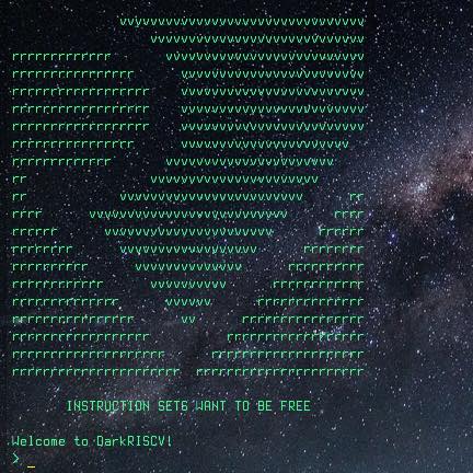
INSTRUCTION SETS WANT TO BE FREE
boot0: text@0 data@4096 stack@8192
board: simulation only (id=0)
build: darkriscv fw build Sat, 30 May 2020 00:55:21 -0300
core0: [email protected] with rv32e+MT+MAC
uart0: 115200 bps (div=868)
timr0: periodic timer=1000000Hz (io.timer=99)
Welcome to DarkRISCV!
> no UART input, finishing simulation...
echo simulation ok.
simulation ok.
make[1]: Leaving directory `/home/marcelo/Documents/Verilog/darkriscv/v38/sim'
make -C boards all BOARD=piswords_rs485_lx9 HARVARD=1
make[1]: Entering directory `/home/marcelo/Documents/Verilog/darkriscv/v38/boards'
cd ../tmp && xst -intstyle ise -ifn ../boards/piswords_rs485_lx9/darksocv.xst -ofn ../tmp/darksocv.syr
Reading design: ../boards/piswords_rs485_lx9/darksocv.prj
*** lots of weird FPGA related messages here ***
cd ../tmp && bitgen -intstyle ise -f ../boards/avnet_microboard_lx9/darksocv.ut ../tmp/darksocv.ncd
echo done.
done.
Which means that the software compiled and liked correctly, the simulation worked correctly and the FPGA build produced a image that can be loaded in your FPGA board with a make install (case you has a FPGA board and, of course, you have a JTAG support script in the board directory).
Case the FPGA is correctly programmed and the UART is attached to a terminal emulator, the FPGA will be configured with the DarkRISCV, which will run the test software and produce the following result:
              vvvvvvvvvvvvvvvvvvvvvvvvvvvvvvvv
                  vvvvvvvvvvvvvvvvvvvvvvvvvvvv
rrrrrrrrrrrrr       vvvvvvvvvvvvvvvvvvvvvvvvvv
rrrrrrrrrrrrrrrr      vvvvvvvvvvvvvvvvvvvvvvvv
rrrrrrrrrrrrrrrrrr    vvvvvvvvvvvvvvvvvvvvvvvv
rrrrrrrrrrrrrrrrrr    vvvvvvvvvvvvvvvvvvvvvvvv
rrrrrrrrrrrrrrrrrr    vvvvvvvvvvvvvvvvvvvvvvvv
rrrrrrrrrrrrrrrr      vvvvvvvvvvvvvvvvvvvvvv
rrrrrrrrrrrrr       vvvvvvvvvvvvvvvvvvvvvv
rr                vvvvvvvvvvvvvvvvvvvvvv
rr            vvvvvvvvvvvvvvvvvvvvvvvv      rr
rrrr      vvvvvvvvvvvvvvvvvvvvvvvvvv      rrrr
rrrrrr      vvvvvvvvvvvvvvvvvvvvvv      rrrrrr
rrrrrrrr      vvvvvvvvvvvvvvvvvv      rrrrrrrr
rrrrrrrrrr      vvvvvvvvvvvvvv      rrrrrrrrrr
rrrrrrrrrrrr      vvvvvvvvvv      rrrrrrrrrrrr
rrrrrrrrrrrrrr      vvvvvv      rrrrrrrrrrrrrr
rrrrrrrrrrrrrrrr      vv      rrrrrrrrrrrrrrrr
rrrrrrrrrrrrrrrrrr          rrrrrrrrrrrrrrrrrr
rrrrrrrrrrrrrrrrrrrr      rrrrrrrrrrrrrrrrrrrr
rrrrrrrrrrrrrrrrrrrrrr  rrrrrrrrrrrrrrrrrrrrrr

       INSTRUCTION SETS WANT TO BE FREE

boot0: text@0 data@4096 stack@8192
board: piswords rs485 lx9 (id=6)
build: darkriscv fw build Fri, 29 May 2020 23:56:39 -0300
core0: [email protected] with rv32e+MT+MAC
uart0: 115200 bps (div=868)
timr0: periodic timer=1000000Hz (io.timer=99)

Welcome to DarkRISCV!
>
The beautiful ASCII RISCV logo was produced by Andrew Waterman! [6]
As long as the build works, it is possible start make changes, but my recommendation when working with soft processors is not work in the hardware and software at the same time! This means that is better freeze the hardware and work only with the software or freeze the software and work only with the hardware. It is perfectly possible make your research in both, but not at the same time, otherwise you find the DarkRISCV in a non-working state after software and hardware changes and you will not be sure where the problem is.
The src directory contains the source code for the test firmware, which includes the boot code, the main process and auxiliary libraries. The code is compiled via gcc in a way that some auxiliary files are produced, for example:
- boot.c: the original C code for the boot process
- boot.s: the assembler version of the C code, generated automatically by the gcc
- boot.o: the compiled version of the C code, generated automatically by the gcc
When all .o files are produced, the result is linked in a darksocv.o ELF file, which is used to produce the darksocv.bin file, which is converted to hexadecimal and separated in ROM and RAM files (which are loaded by the Verilog code in the blockRAMs). The linker also produces a darksocv.lst with a complete list of the code generated and the darsocv.map, which shows the map of all functions and variables in the produced code.
The firmware concept is very simple:
- boot.c contains the boot code
- main.c contains the main application code (shell)
- banner.c contains the riscv banner
- stdio.c contains a small version of stdio
- io.c contains the IO interfaces
Extra code can be easily added in the compilation by editing the src/Makefile.
For example, in order to add a lempel-ziv code lz.c, it is necessary make the Makefile knows that we need the lz.s and lz.o:
OBJS = boot.o stdio.o main.o io.o banner.o lz.o
ASMS = boot.s stdio.s main.s io.s banner.s lz.s
SRCS = boot.c stdio.c main.c io.c banner.c lz.c
And add a "lz" command in the main.c, in a way that is possible call the function via the prompt. Alternatively, it is possible entirely replace the provided firmware and use your own firmware.
The simulation, in the other hand will show some waveforms and is possible check the DarkRISCV operation when running the example code.
The main simulation tool for DarkRISCV is the iSIM from Xilinx ISE 14.7, but the Icarus simulator is also supported via the Makefile in the sim directory (the changes regarding Icarus are active when the symbol ICARUS is detected). I also included a workaround for ModelSim, as pointed by our friend HYF (the changes regarding ModelSim are active when the symbol MODEL_TECH is detected).
The simulation runs the same firmware as in the real FPGA, but in order to improve the simulation performance, the UART code is not simulated, since the 115200 bps requires lots dead simulation time.
The RTL directory contains the DarkRISCV core and some auxiliary files, such as the DarkSoCV (a small system-on-chip with ROM, RAM and IO), the DarkUART (a small UART for debug) and the configuration file, where is possible enable and disable some features that are described in the Implementation Notes section.
The current supported boards are:
- id==0 simulation only
- id==1 avnet_microboard_lx9
- id==2 xilinx_ac701_a200
- id==3 qmtech_sdram _lx16
- id==4 qmtech_spartan7_s15
- id==5 lattice_brevia2_lxp2
- id==6 piswords_rs485_lx9
- id==7 digilent_spartan3_s200
- id==8 aliexpress_hpc40gbe k420
- id==9 qmtech_artix7_a35
- id==10 aliexpress_hpc40gbe_ku040
- id==11 papilio_duo_logicstart
- id==12 qmtech_kintex7_k325
- id==13 scarab_minispartan6-plus_lx9
- id==14 colorlighti9_ecp5-45f
- id==15 colorlighti5_ecp5-25f
- id==16 ulx3s_ecp5-85f
The organization is self-explained, w/ the vender, board and FPGA model in the name of the directory. Each board directory contains the project files to be open in the Xilinx ISE 14.x, as well Makefiles to build the FPGA image regarding that board model. Although a ucf file is provided in order to generate a complete build with a UART and some LEDs, the FPGA is NOT fully wired in any particular configuration and you must add the pins that you will use in your FPGA board.
Anyway, although not wired, the build always gives you a good estimation about the FPGA utilization and about the timing (because the UART output ensures that the complete processor must be synthesized).
As long there are much supported boards, there is no way to test all boards everytime, which means that sometimes the changes regarding one board may affect other board in a wrong way.
[*This section is kept for reference, but the description may not match exactly with the current code]
Since my target is the ultra-low-cost Xilinx Spartan-6 family of FPGAs, the project is currently based in the Xilinx ISE 14.7 for Linux, which is the latest available ISE version. However, there is no explicit reference for Xilinx elements and all logic is inferred directly from Verilog, which means that the project is easily portable to other FPGA families and easily portable to other environments, as can be observed in the case of Lattice XP2 support. Anyway, keep in mind that certain Verilog structures may not work well in some FPGAs.
In the last update I included a way to test the firmware in the x86 host, which helps as lot, since is possible interact with the firmware and fix quickly some obvious bugs. Of course, the x86 code does not run the boot.c code, since makes no sense (?) run the RISCV boot code in the x86.
Anyway, as main recomendation when working with softcores try never work in the hardware and in the software at the same time! Start with the minimum software configuration possible and freeze the software. When implementing new software updates, use the minium hardware configuration possible and freeze the hardware.
The RV32I specification itself is really impressive and easy to implement (see [1], page 16). Of course, there are some drawbacks, such as the funny little-endian bus (opposed to the network oriented big-endian bus found in the 680x0 family), but after some empirical tests it is easy to make work.
The funny information here is that, after lots of research regarding add support for big-endian in the DarkRISCV, I found no way to make the GCC generate the code and data correctly.
Another drawback in the specification is the lacking of delayed branches. Although i understand that they are bad from the conceptual point of view, they are good trick in order to extract more performance. As reference, the lack of delayed branches or branch predictor in the DarkRISCV may reduce between 20 and 30% the performance, in a way that the real measured performance may be between 1.25 and 1.66 clocks per instruction.
Although the branch prediction is not complex to implement, I found the experimental multi-threading support far more interesting, as long enable use the idle time in the branches to swap the processor thread. Anyway, I will try debug the branch prediction code in order to improve the single-thread performance.
The core supports 2 or 3-state pipelines and, although the main logic is almost the same, there are huge difference in how they works. Just for reference, the following section reflects the historic evolution of the core and may not reflect the current core code.
The original 2-stage pipeline design has a small problem concerning the ROM and RAM timing, in a way that, in order to pre-fetch and execute the instruction in two clocks and keep the pre-fetch continously working at the rate of 1 instruction per clock (and the same in the execution), the ROM and RAM must respond before the next clock. This means that the memories must be combinational or, at least, use a 2-phase clock.
The first solution for the 2-stage pipeline version with a 2-phase clock is the default solution and makes the DarkRISCV work as a pseudo 4-stage pipeline:
- 1/2 stage for instruction pre-fetch (rom)
- 1/2 stage for static instruction decode (core)
- 1/2 stage for address generation, register read and data read/write (ram)
- 1/2 stage for data write (register write)
From the processor point of view, there are only 2 stages and from the memory point of view, there are also 2 stages. But they are in different clock phases. In normal conditions, this is not recommended because decreases the performance by a 2x factor, but in the case of DarkRISCV the performance is always limited by the combinational logic regarding the instruction execution.
The second solution with a 2-stage pipeline is use combinational logic in order to provide the needed results before the next clock edge, in a way that is possible use a single phase clock. This solution is composed by a instruction and data caches, in a way that when the operand is stored in a small LUT-based combinational cache, the processor can perform the memory operation with no extra wait states. However, when the operand is not stored in the cache, extra wait-states are inserted in order to fetch the operand from a blockram or extenal memory. According to some preliminary tests, the instruction cache w/ 64 direct mapped instructions can reach a hit ratio of 91%. The data cache performance, although is not so good (with a hit ratio of only 68%), will be a requirement in order to access external memory and reduce the impact of slow SDRAMs and FLASHes.
Unfortunately, the instruction and data caches are not working anymore for the 2-stage pipeline version and only the instruction cache is working in the 3-stage pipeline. The problem is probably regarding the HLT signal and/or a problem regarding the write byte enable in the cache memory.
Both the use of the cache and a 2-phase clock does not perform well. By this way, a 3-stage pipeline version is provided, in order to use a single clock phase with blockrams.
The concept in this case is separate the pre-fetch and decode, in a way that the pre-fetch can be done entirely in the blockram side for the instruction bus. The decode, in a different stage, provides extra performance and the execute stage works with one clock almost all the time, except when the load instruction is executed. In this case, the external memory logic inserts one wait-state. The write operation, however, is executed in a single clock.
The solution with wait-states can be used in the 2-stage pipeline version, but decreases the performance too much. Case is possible run all versions with the same, clock, the theorical performance in clocks per instruction CPI), number of clocks to flush the pipeline in the taken branch (FLUSH) and memory wait-states (WSMEM) will be:
- 2-stage pipe w/ 2-phase clock: CPI=1, FLUSH=1, WSMEM=0: real CPI=~1.25
- 3-stage pipe w/ 1-phase clock: CPI=1, FLUSH=2, WSMEM=1: real CPI=˜1.66
- 2-stage pipe w/ 1-phase clock: CPI=2, FLUSH=1, WSMEM=1, real CPI=~2.00
Empiracally, the impact of the FLUSH in the 2-stage pipeline is around 20% and in the 3-stage pipeline is 30%. The real impact depends of the code itself, of course... In the case of the impact of the wait-states in the memory access regarding the load instruction, the impact ranges between 5 and 10%, again, depending of the code.
However, the clock in the case of the 3-stage pipeline is far better than the 2-stage pipeline, in special because the better distribuition of the logic between the decode and execute stages.
Currently, the most expensive path in the Spartan-6 is the address bus for the data side of the core (connected to RAM and peripherals). The problem regards to the fact that the following actions must be done in a single clock:
- generate the DADDR[31:0] = REG[SPTR][31:0]+EXTSIG(IMM[11:0])
- generate the BE[3:0] according to the operand size and DADDR[1:0]
In the case of read operation, the DATAI path includes also a small mux in order to separate RAM and peripheral buses, as well separate the diferent peripherals, which means that the path increases as long the number of peripherals and the complexity increases.
Of course, the best performance setup uses a 3-state pipeline and a single-clock phase (posedge) in the entire logic, in a way that the 2-stage pipeline and dual-clock phase will be kept only for reference.
The only disadvantage of the 3-state pipeline is one extra wait-state in the load operation and the longer pipeline flush of two clocks in the taken branches.
Just for reference, I registered some details regarding the performance measurements:
The current firmware example runs in the 3-stage pipeline version clocked at 100MHz runs at a verified performance of 62 MIPS. The theorical 100MIPS performance is not reached 5% due to the extra wait-state in the load instruction and 32% due to pipeline flushes after taken branches. The 2-stage pipeline version, in the other side, runs at a verified performance of 79MIPS with the same clock. The only loss regards to 20% due to pipeline flushes after a taken branch.
Of course, the impact of the pipeline flush depends also from the software and, as long the software is currently optimized for size. When compiled with the -O2 instead of -Os, the performance increase to 68MIPS in the 3-state pipeline and the loss changed to 6% for load and 25% for the pipeline flush. The -O3 option resulted in 67MIPS and the best result was the -O1 option, which produced 70MIPS in the 3-stage version and 85MIPS in the 2-stage version.
By this way, case the performance is a requirement, the src/Makefile must be changed in order to use the -O1 optimization instead of the -Os default.
And although the 2-stage version is 15% faster than the 3-stage version, the 3-stage version can reach better clocks and, by this way, will provide better performance.
Regarding the pipeline flush, it is required after a taken branch, as long the RISCV does not supports delayed branches. The solution for this problem is implement a branch cache (branch predictor), in a way that the core populates a cache with the last branches and can predict the future branches. In some inicial tests, the branch prediction with a 4 elements entry appers to reach a hit ratio of 60%.
Another possibility is use the flush time to other tasks, for example handle interrupts. As long the interrupt handling and, in a general way, threading requires flush the current pipelines in order to change context, by this way, match the interrupt/threading with the pipeline flush makes some sense!
With the option THREADING is possible test this feature.
The implementation is in very early stages of development and does not handle correctly the initial SP and PC. Anyway, it works and enables the main() code stop in a gets() while the interrupt handling changes the GPIO at a rate of more than 1 million interrupts per second without affecting the execution and with little impact in the performance! :)
The interrupt support can be expanded to a more complete threading support, but requires some tricks in the hardware and in the software, in order to populate the different threads with the correct SP and PC.
The interrupt handling use a concept around threading and, with some extra effort, it is probably possible support 4, 8 or event 16 threads. The drawback in this case is that the register bank increses in size, which explain why the rv32e is an interesting option for threading: with half the number of registers is possible store two more threads in the core.
Currently, the time to switch the context in the darkricv is two clocks in the 3-stage pipeline, which match with the pipeline flush itself. At 100MHz, the maximum empirical number of context switches per second is around 2.94 million.
NOTE: the interrupt controller is currently working only with the -Os flag in the gcc!
About the new MAC instruction, it is implemented in a very preliminary way with the OPCDE 7'b1111111 (this works, but it is a very bad decision!). I am checking about the possibility to use the p.mac instruction, but at this time the instruction is hand encoded in the mac() function available in the stdio.c (i.e. the darkriscv libc). The details about include new instructions and make it work with GCC can be found in the reference [5].
The preliminary tests pointed, as expected, that the performance decreases to 90MHz and although it was possible run at 100MHz with a non-zero timing score and reach a peak performance of 100MMAC/s, the small 32-bit accumulator saturates too fast and requries extra tricks in order to avoid overflows.
The mul operation uses two 16-bit integers and the result is added with a separate 32-bit register, which works as accumulator. As long the operation is always signed and the signal always use the MSB bit, this means that the 15x15 mul produces a 30 bit result which is added to a 31-bit value, which means that the overflow is reached after only two MAC operations.
In order to avoid overflows, it is possible shift the input operands. For example, in the case of G711 w/ u-law encoding, the effective resolution is 14 bits (13 bits for integer and 1 bit for signal), which means that a 13x13 bit mul will be used and a 26-bit result produced to be added in a 31-bit integer, enough to run 32xMAC operations before overflow (in this case, when the ACC reach a negative value):
# awk 'BEGIN { ACC=2**31-1; A=2**13-1; B=-A; for(i=0;ACC>=0;i++) print i,A,B,A*B,ACC+=A*B }'
0 8191 -8191 -67092481 2080391166
1 8191 -8191 -67092481 2013298685
2 8191 -8191 -67092481 1946206204
...
30 8191 -8191 -67092481 67616736
31 8191 -8191 -67092481 524255
32 8191 -8191 -67092481 -66568226
Is this theory correct? I am not sure, but looks good! :)
As complement, I included in the stdio.c the support for the GCC functions regarding the native *, / and % (mul, div and mod) operations with 32-bit signed and unsigned integers, which means true 32x32 bit operations producing 32-bit results. The code was derived from an old 68000-related project (as most of code in the stdio.c) and, although is not so faster, I guess it is working. As long the MAC instruction is better defined in the syntax and features, I think is possible optimize the mul/div/mod in order to try use it and increase the performance.
Here some additional performance results (synthesis only, 3-stage version) for other Xilinx devices available in the ISE for speed grade 2:
- Spartan-6: 100MHz (measured 70MIPS w/ gcc -O1)
- Artix-7: 178MHz
- Kintex-7: 225MHz
For speed grade 3:
- Spartan-6: 117MHz
- Artix-7: 202MHz
- Kintex-7: 266MHz
The Kintex-7 can reach, theorically 186MIPS w/ gcc -O1.
This performance is reached w/o the MAC and THREADING activated. Thanks to the RV32E option, the synthesis for the Spartan-3E is now possible with resulting in 95% of LUT occupation in the case of the low-cost 100E model and 70MHz clock (synthesis only and speed grade 5):
- Spartan-3E: 70MHz
For the 2-stage version and speed grade 2, we have less impact from the pipeline flush (20%), no impact in the load and some impact in the clock due to the use of a 2-phase clock:
- Spartan-6: 56MHz (measured 47MIPS w/ -O1)
About the compiler performance, from boot until the prompt, tested w/ the 3-stage pipeline core at 100MHz and no interrupts, rom and ram measured in 32-bit words:
- gcc w/ -O3: t=289us rom=876 ram=211
- gcc w/ -O2: t=291us rom=799 ram=211
- gcc w/ -O1: t=324us rom=660 ram=211
- gcc w/ -O0: t=569us rom=886 ram=211
- gcc w/ -Os: t=398us rom=555 ram=211
Due to reduced ROM space in the FPGA, the -Os is the default option.
In another hand, regarding the support for Vivado, it is possible convert the Artix-7 (Xilinx AC701 available in the ise/boards directory) project to Vivado and make some interesting tests. The only problem in the conversion is that the UCF file is not converted, which means that a new XDC file with the pin description must be created.
The Vivado is very slow compared to ISE and needs lots of time to synthesise and inform a minimal feedback about the performance... but after some weeks waiting, and lots of empirical calculations, I get some numbers for speed grade 2 devices:
- Artix7: 147MHz
- Spartan-7: 146MHz
And one number for speed grade 3 devices:
- Kintex-7: 221MHz
Although Vivado is far slow and shows pessimistic numbers for the same FPGAs when compared with ISE, I guess Vivado is more realistic and, at least, it supports the new Spartan-7, which shows very good numbers (almost the same as the Artix-7!).
That values are only for reference. The real values depends of some options in the core, such as the number of pipeline stages, who the memories are connected, etc. Basically, the best clock is reached by the 3-stage pipeline version (up to 100MHz in a Spartan-6), but it requires at lease 1 wait state in the load instruction and 2 extra clocks in the taken branches in order to flush the pipeline. The 2-state pipeline requires no extra wait states and only 1 extra clock in the taken branches, but runs with less performance (56MHz).
Well, my conclusion after some years of research is that the branch prediction solve lots of problems regarding the performance.
About the gcc compiler, I am working with the experimental gcc 9.0.0 for RISC-V. No patches or updates are required for the DarkRISCV other than the -march=rv32i. Although the fence*, e* and crg* instructions are not implemented, the gcc appears to not use of that instructions and they are not available in the core.
Although is possible use the compiler set available in the oficial RISC-V site, our colleagues from lowRISC project pointed a more clever way to build the toolchain:
Basically:
git clone --depth=1 git://gcc.gnu.org/git/gcc.git gcc
git clone --depth=1 git://sourceware.org/git/binutils-gdb.git
git clone --depth=1 git://sourceware.org/git/newlib-cygwin.git
mkdir combined
cd combined
ln -s ../newlib-cygwin/* .
ln -sf ../binutils-gdb/* .
ln -sf ../gcc/* .
mkdir build
cd build
../configure --target=riscv32-unknown-elf --enable-languages=c --disable-shared --disable-threads --disable-multilib --disable-gdb --disable-libssp --with-newlib --with-arch=rv32ima --with-abi=ilp32 --prefix=/usr/local/share/gcc-riscv32-unknown-elf
make -j4
make
make install
export PATH=$PATH:/usr/local/share/gcc-riscv32-unknown-elf/bin/
riscv32-unknown-elf-gcc -v
and everything will magically work! (:
Case you have no succcess to build the compiler, have no interest to change the firmware or is just curious about the darkriscv running in a FPGA, the project includes the compiled ROM and RAM, in a way that is possible examine all derived objects, sources and correlated files generated by the compiler without need compile anything.
Finally, as long the DarkRISCV is not yet fully tested, sometimes is a very good idea compare the code execution with another stable reference!
In this case, I am working with the project picorv32:
https://github.com/cliffordwolf/picorv32
When I have some time, I will try create a more well organized support in order to easily test both the DarkRISCV and picorv32 in the same cache, memory and IO sub-systems, in order to make possible select the core according to the desired features, for example, use the DarkRISCV for more performance or picorv32 for more features.
About the software, the most complex issue is make the memory design match with the linker layout. Of course, it is a gcc issue and it is not even a problem, in fact, is the way that the software guys works when linking the code and data!
In the most simplified version, directly connected to blockRAMs, the DarkRISCV is a pure harvard architecture processor and will requires the separation between the instruction and data blocks!
When the cache controller is activated, the cache controller provides separate memories for instruction and data, but provides a interface for a more conventional von neumann memory architecture.
In both cases, a proper designed linker script (darksocv.ld) probably solves the problem!
The current memory map in the linker script is the follow:
- 0x00000000: 4KB ROM
- 0x00001000: 4KB RAM
Also, the linker maps the IO in the following positions:
- 0x80000000: UART status
- 0x80000004: UART xmit/recv buffer
- 0x80000008: LED buffer
The RAM memory contains the .data area, the .bss area (after the .data and initialized with zero), the .rodada and the stack area at the end of RAM.
Although the RISCV is defined as little-endian, appears to be easy change the configuration in the GCC. In this case, it is supposed that the all variables are stored in the big-endian format. Of course, the change requires a similar change in the core itself, which is not so complex, as long it affects only the load and store instructions. In the future, I will try test a big-endian version of GCC and darkriscv, in order to evaluate possible performance enhancements in the case of network oriented applications! :)
Finally, the last update regarding the software included new option to build a x86 version in order to help the development by testing exactly the same firmware in the x86.
In a preliminary way, it is possible build the gcc for RV32E with the folllowing configuration:
git clone --depth=1 git://gcc.gnu.org/git/gcc.git gcc
git clone --depth=1 git://sourceware.org/git/binutils-gdb.git
git clone --depth=1 git://sourceware.org/git/newlib-cygwin.git
mkdir combined
cd combined
ln -s ../newlib-cygwin/* .
ln -sf ../binutils-gdb/* .
ln -sf ../gcc/* .
mkdir build
cd build
../configure --target=riscv32-embedded-elf --enable-languages=c --disable-shared --disable-threads --disable-multilib --disable-gdb --disable-libssp --with-newlib  --with-arch-rv32e --with-abi=ilp32e --prefix=/usr/local/share/gcc-riscv32-embedded-elf
make -j4
make
make install
export PATH=$PATH:/usr/local/share/gcc-riscv32-embedded-elf/bin/
riscv32-embedded-elf-gcc -v
Currently, I found no easy way to make the GCC build big-endian code for RISCV. Instead, the easy way is make the endian switch directly in the IO device or in the memory region.
As long is not so easy build the GCC in some machines, I left in a public share the source and the pre-compiled binary set of GCC tools for RV32E:
https://drive.google.com/drive/folders/1GYkqDg5JBVeocUIG2ljguNUNX0TZ-ic6?usp=sharing
As far as i remember it was compiled in a Slackware Linux or something like, anyway, it worked fine in the Windows 10 w/ WSL and in other linux-like environments.
Currently, the following boards are supported:
- Avnet Microboard LX9: equipped with a Xilinx Spartan-6 LX9 running at 100MHz
- XilinX AC701 A200: equipped with a Xilinx Artix-7 A200 running at 90MHz
- QMTech SDRAM LX16: equipped with a Xilinx Spartan-6 LX16 running at 100MHz
- QMTech NORAM S15: equipped with a Xilinx Spartan-7 S15 running at 100MHz
- Lattice Brevia2 XP2: equipped with a Lattice XP2-6 running at 50MHz
- Piswords RS485 LX9: equipped with a Xilinx Spartan-6 LX9 running at 100MHz
- Digilent S3 Starter Board: equipped with a Xilinx Spartan-3 S200 running at 50MHz
The speeds are related to available clocks in the boards and different clocks may be generated by programming a clock generator. The Spartan-6 is found in most boards and the core runs fine at ~100MHz, regardless the frequency of the main oscillator (typically 50MHz).
All Xilinx based boards typically supports a 115200 bps UART for console, some LEDs for debug and on-chip 4KB ROM and 4KB RAM (as well the RESET button to restart the core and the DEBUG signals for an oscilloscope).
In the case of QMTECH boards, that does not include the JTAG neither the UART/USB port, and external USB/UART converter and a low-cost JTAG adapter can solve the problem easily!
The Lattice Brevia is clocked by the on-board 50MHz oscillator, with the UART operating at 115200bps and the LED and DEBUG ports wired to the on- board LEDs.
Although the Digilent Spartan-3 Starter Board, this is a very useful board to work as reference for LUT4 technology, in a way that is possible improve the support in the future for alternative low-cost LUT4 FPGAs.
In the software side, a small shell is available with some basic commands:
- clear: clear display
- dump : dumps an area of the RAM
- led : change the LED register (which turns on/off the LEDs)
- timer : change the timer prescaler, which affects the interrupt rate
- gpio : change the GPIO register (which changes the DEBUG lines)
The proposal of the shell is provide some basic test features which can provide a go/non-go status about the current hardware status.
Useful memory areas:
- 4096: the start of RAM (data)
- 4608: the start of RAM (data)
- 5120: empty area
- 5632: empty area
- 6144: empty area
- 6656: empty area
- 7168: empty area
- 7680: the end of RAM (stack)
As long the DarkRISCV uses separate instruction and data buses, it is not possible dump the ROM area. However, this limitation is not present when the option HARVARD is activated, as long the core is constructed in a way that the ROM bus is conected to one bus from a dual-ported memory and the RAM bus is connected to a different bus from the same dual-ported memory. From the DarkRISCV point of view, they are fully separated and independent buses, but in reality they area in the same memory area, which makes possible the data bus change the area where the code is stored. With this feature, it will be possible in the future create loadable codes from the FLASH memory! :)
Last xmas (2022) our colleague Lucas Teske added support for FuseSoC in the darkriscv... I am not much aware how it works and how use it, but it is supposed to handle the build tools automatically! It is the same tool used by SERV and I used it to add some kilocore records in the past... in order to make it work in the darkriscv, please try:
- fusesoc run --target=qmtech_artix7_a35 darklife:darkriscv:darksocv
At this moment, not all boards are really supported yet. Supported boards are:
- Colorlight i9
- Colorlight i5
- Lattice iCE40 Devkit
- QMtech Artix 7 (Vivado)
I found that some people are very reticent about the possibility of designing a RISC-V processor in one night. Of course, it is not so easy as it appears and, in fact, it require a lot of experience, planning and luck. Also, the fact that the processor correctly run some few instructions and put some garbage in the serial port does not really means that the design is perfect, instead you will need lots and lots of debug time in order to fix all hidden problems.
Just in case, I found a set of online videos from my friend (Lucas Teske) that shows the design of a RISC-V processor from scratch (playlist with 9 videos):
Alternatively, there are the original videos in the twitch:
- https://www.twitch.tv/videos/840983740 Register bank (4h50)
- https://www.twitch.tv/videos/845651672 Program counter and ALU (3h49)
- https://www.twitch.tv/videos/846763347 ALU tests, CPU top level (3h47)
- https://www.twitch.tv/videos/848921415 Computer problems and microcode planning (08h19)
- https://www.twitch.tv/videos/850859857 instruction decode and execute - part 1/3 (08h56)
- https://www.twitch.tv/videos/852082786 instruction decode and execute - part 2/3 (10h56)
- https://www.twitch.tv/videos/858055433 instruction decode and execute - part 3/3 - SoC simulation (10h24)
- TBD tests in the Lattice FPGA
- TBD tests in the Lattice FPGA w/ LCD display
Unfortunately the video set is currently in portuguese only and there a lot of parallel discussions about technology, including the fix of the Teske's notebook online! I hope in the future will be possible edit the video set and, maybe, create english subtitles.
About the processor itself, it is a microcode oriented concept with a classic von neumann archirecture, designed to support more easily different ISAs. It is really very different than the traditional RISC cores that we found around! Also, it includes a very good eco-system around opensource tools, such as Icarus, Yosys and gtkWave!
Although not finished yet (95% done!), I think it is very illustrative about the RISC-V design:
- rv32e instruction set: very reduced (37) and very ortogonal bit patterns (6)
- rv32e register set: 16x32-bit register bank and a 32-bit program counter
- rv32e ALU with basic operations for reg/imm and reg/reg instructions
- rv32e instruction decode: very simple to understand, very direct to implement
- rv32e software support: the GCC support provides an easy way to generate code and test it!
The Teske's proposal is not design the faster RISC-V core ever (we already have lots of faster cores with CPI ~ 1, such as the darkriscv, vexriscv, etc), but create a clean, reliable and compreensive RISC-V core.
You can check the code in the following repository:
In a funny way, the DarkRISCV appears in some academic papers, sometimes in a comparative way, sometimes as a laboratory mouse.
-
Design and Implementation of a 256-Bit RISC-V-Based Dynamically Scheduled Very Long Instruction Word on FPGA -- Here we found an interesting comparison between the DarkRISCV versus a huge 8-way VLIW core, as well the Kronos RISCV, the PicoRV32 and the NEORV32. Nice results for DarkRISCV: 2nd place w/ IPC 0.71 and 1st place with only 1500LUTs. https://ieeexplore.ieee.org/iel7/6287639/8948470/09200617.pdf
-
ReCon: From the Bitstream to Piracy Detection -- Interesting paper about IP piracy detection, basically how detect an IP inside an bitstream, they used the PicoRV32, OpenRISC and DarkRISCV as IPs to be detected. https://homes.luddy.indiana.edu/lukefahr/papers/skipper_paine20.pdf
-
A Low-Cost Fault-Tolerant RISC-V Processor for Space Systems -- Here we found an interesting comparison between low-cost RISCV cores, but in this case the DarkRISCV performs very badly against the PicoRV32, mRISCV, Ibex and a radiation hardned RISCV core. Not sure about the tools and the target, as long I have no access to the paper, just some pictures. https://www.semanticscholar.org/paper/A-Low-Cost-Fault-Tolerant-RISC-V-Processor-for-Santos-Luza/b8cd0b62ac914678f1999df09a4b77b857178d33
-
Fault Classification and Vulnerability Analysis of Microprocessors -- No much information, since the paper will released only in 2022, but the abstract is very interesting, basically they will inject lots of faults in the PicoRV32 and DarkRISCV in order to see what happens. https://repository.tudelft.nl/islandora/object/uuid:4c85a1ba-2721-4563-bb13-31d506d9c906?collection=education
Regarding real world applications, standard embbeded C code typically runs very well with DarkRISCV. Some examples of applications currently in use:
- microcontroller programmers (JTAG and other complex protocols)
- data compression/decompression (LZ streams)
- cryptography (RSA and SHA256, requires hardware accelerators)
- digital signal processing (requires mac instruction)
In the case of RSA, the simple inclusion of a pipelined 32x32-bit multiplier mapped via IO (i.e. not the M extension, instead an IO mapped register accessible via load/store instructions) increased the RSA performance by a factor of 20x when compared to the bare RV32E instruction set. In the case of SHA256, a complete SHA256 accelerator in hardware and mapped via IO can transfor seconds of processing in few miliseconds. In both cases, no need for complex instruction integration in the core, no need to wait -- the core and the accelerator can work in parallel.
I tried prepare a fair performance comparison between the DarkRISCV and different FPGAs, but it is not so easy as it appears! The first problem is locate HDL versions of each core, since the tools require verilog or VHDL files in order to build something. The second problem is decide what compile: there are lots of combinations of top level blocks, with different peripherals and concepts. In this case, I included only the core. The third problem regards to the core configuration: it is not easy or clear how to configure them to the minimum area or maximum speed, so I just used the default configuration for all cores. In short words, I solved the problem in a dummy way (which reflects the reality in 95% of time).
As long I have separate builds for each core, there is the final problem: how analyse the results and rank the cores. My option was calculate how many MIPS is possible in a fixed FPGA, in this case the Kintex-7 K420 with 260600 LUTs of 6-inputs. Different cores will require different amount of LUTs, just divide the total number by the required ammount and we have the theorical number of cores per FPGA (peak cores/FPGA). Also, different cores have different theorical peak IPC. guessed numbers and, according to the synthesis tool in the default setup, will run at different maximum frequencies. As long we know the number of instruction per clock and the maximum number of clocks per second (the maximum frequency), we have the maximum number of instructions per second (peak MIPS) per core. As long we also knows about the maximum number of cores, we can calculate the maximum peak MIPS per FPGA.
The following list is far from complete, but it is my suggestion to compare different cores:
Core		LUT	FF	DSP	BRAM	IPC	MFreq	Ncores	MIPS/k7	REPO
DarkRISCV	1177	246	0	0	1	150	221	33232	https://github.com/darklife/darkriscv
VexRISCV	1993	1345	4	5	1	214	130	28013	https://github.com/m-labs/VexRiscv-verilog
PicoRV32	1291	568	0	1	1/4	309	201	15630	https://github.com/cliffordwolf/picorv32
SERV		217	174	0	0	1/32	367	1200	13788	https://github.com/olofk/serv
RPU		2943	1103	12	1	1	111	88	9905	https://github.com/Domipheus/RPU
UE RISC-V	3676	2289	4	0	1	124	70	8811	https://github.com/ultraembedded/riscv
UE BiRISC-V	15667	6324	4	0	2	87	16	2917	https://github.com/ultraembedded/biriscv
Are that results fair enough? from my point of view, as long the conditions are the same, yes. Are that results true enough? from my point of view, maybe. At least two cases does not match: the DarkRISCV reaches up to 240MHz in the same FPGA when the top level is in the build. Not sure why the core only result in smaller maximum frequency, but the point is try to find a way to compare different cores, so it is okay. The second case is the SERV, which shows a maximum frequency of 367MHz and up to 1200 cores/FPGA. In fact, I tested up to 1000 SERV cores in that FPGA and appears to be possivel fit between 1100 and 1200 cores as result of optimizations across the multi-core hierarchy. The bad news is that the maximum clock barely reached 128MHz per core. Again, the point is try to find a way to compare differnt cores, so it is okay.
For sure that numbers will be very useful for future designers and the message is clear: keep it simple! Less area per core means more cores in the same area and, in some cases, means better performance. In most cases, less are also means better clock performance, but in this case the better clock is useful only when the IPC is around 1, which is not so easy to keep. Just as example, the DarkRISCV can trully reach the IPC ~ 1, but the code must be optimized by hand and the top level must be changed in a way that there is no latency regarding the BRAM. In a more general way, with less effort, the compiler and a more standard top level can keep the IPC around 0.7, which is good enough for most applications. So, keep your expectives very, very low! :)
Special thanks to my old colleagues from the Verilog/VHDL/IT area:
- Paulo Matias (jedi master and verilog/bluespec/riscv guru)
- Paulo Bernard (co-worker and verilog guru)
- Evandro Hauenstein (co-worker and git guru)
- Lucas Mendes (technology guru)
- Marcelo Toledo (technology guru)
- Fabiano Silos (technology guru)
Also, special thanks to the "friends of darkriscv" that found the project in the internet and contributed in any way to make it better:
- Guilherme Barile (technology guru and first guy to post anything about the darkriscv! [2]).
- Alasdair Allan (technology guru, posted an article about the darkriscv [3])
- Gareth Halfacree (technology guru, posted an article about the DarkRISCV [4])
- Ivan Vasilev (ported DarkRISCV for Lattice Brevia XP2!)
- timdudu from github (fix in the LDATA and found a bug in the BCC instruction)
- hyf6661669 from github (lots of contributions, including the fixes regarding the AUIPC and S{B,W,L} instructions, ModelSIM simulation, the memory byte select used by store/load instructions and much more!)
- zmeiresearch from github (support for Lattice XP2 Brevia board)
- All other colleagues from github that contributed with fixes, corrections and suggestions.
Finally, thanks to all people who directly and indirectly contributed to this project, including the company I work for and all colleagues that tested the DarkRISCV.
[1] https://www.amazon.com/RISC-V-Reader-Open-Architecture-Atlas/dp/099924910X
[2] https://news.ycombinator.com/item?id=17852876
[3] https://blog.hackster.io/the-rise-of-the-dark-risc-v-ddb49764f392
[4] https://abopen.com/news/darkriscv-an-overnight-bsd-licensed-risc-v-implementation/
[5] http://quasilyte.dev/blog/post/riscv32-custom-instruction-and-its-simulation/
[6] https://github.com/riscv/riscv-pk/blob/master/bbl/riscv_logo.txt